Component Reference
Lumped Components
Widerstand
Symbol

Component Data
| Field | Wert |
|---|---|
| Caption | Widerstand |
Beschreibung |
Widerstand |
| Schematic entry | R |
| Netlist entry | R |
Typ |
AnalogComponent |
| Bitmap file | Widerstand |
Eigenschaften |
6 |
| Category | lumped components |
Component Parameters
| Name | Wert |
Display | Beschreibung |
|---|---|---|---|
| R | 50 Ohm | ja |
Ohmscher Widerstand in Ohm |
| Temp | 26.85 | nein |
Simulationstemperatur in °C |
| Tc1 | 0.0 | nein |
Temperaturkoeffizient erster Ordnung |
| Tc2 | 0.0 | nein |
Temperaturkoeffizient zweiter Ordnung |
| Tnom | 26.85 | nein |
Temperatur bei der die Modellparameter extrahiert wurden |
| Symbol | european | nein |
schematic symbol [european, US] |
Resistor Us
Symbol

Component Data
| Field | Wert |
|---|---|
| Caption | Widerstand US |
Beschreibung |
Widerstand |
| Schematic entry | R |
| Netlist entry | R |
Typ |
AnalogComponent |
| Bitmap file | resistor_us |
Eigenschaften |
6 |
| Category | lumped components |
Component Parameters
| Name | Wert |
Display | Beschreibung |
|---|---|---|---|
| R | 50 Ohm | ja |
Ohmscher Widerstand in Ohm |
| Temp | 26.85 | nein |
Simulationstemperatur in °C |
| Tc1 | 0.0 | nein |
Temperaturkoeffizient erster Ordnung |
| Tc2 | 0.0 | nein |
Temperaturkoeffizient zweiter Ordnung |
| Tnom | 26.85 | nein |
Temperatur bei der die Modellparameter extrahiert wurden |
| Symbol | US | nein |
schematic symbol [european, US] |
Kondensator
Symbol

Component Data
| Field | Wert |
|---|---|
| Caption | Kondensator |
Beschreibung |
Kondensator |
| Schematic entry | C |
| Netlist entry | C |
Typ |
AnalogComponent |
| Bitmap file | Kondensator |
Eigenschaften |
3 |
| Category | lumped components |
Component Parameters
| Name | Wert |
Display | Beschreibung |
|---|---|---|---|
| C | 1 pF | ja |
Kapazität in Farad |
| V | nein |
initial voltage for transient simulation | |
| Symbol | neutral | nein |
schematic symbol [neutral, polar] |
Spule
Symbol

Component Data
| Field | Wert |
|---|---|
| Caption | Spule |
Beschreibung |
Spule |
| Schematic entry | L |
| Netlist entry | L |
Typ |
AnalogComponent |
| Bitmap file | Spule |
Eigenschaften |
2 |
| Category | lumped components |
Component Parameters
| Name | Wert |
Display | Beschreibung |
|---|---|---|---|
| L | 1 nH | ja |
Induktivität in Henry |
| I | nein |
initial current for transient simulation |
Masse
Symbol

Component Data
| Field | Wert |
|---|---|
| Caption | Masse |
Beschreibung |
Masse (Referenzpotential) |
| Schematic entry | GND |
| Netlist entry | |
Typ |
Component |
| Bitmap file | gnd |
Eigenschaften |
0 |
| Category | lumped components |
Schaltkreis-Anschluss
Symbol

Component Data
| Field | Wert |
|---|---|
| Caption | Schaltkreis-Anschluss |
Beschreibung |
Teilschaltungstor |
| Schematic entry | Port |
| Netlist entry | P |
Typ |
Component |
| Bitmap file | subport |
Eigenschaften |
2 |
| Category | lumped components |
Component Parameters
| Name | Wert |
Display | Beschreibung |
|---|---|---|---|
| Num | 1 | ja |
Tornummer in der Teilschaltung |
Typ |
analog | nein |
type of the port (for digital simulation only) [analog, in, out, inout] |
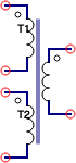
Transformator
Symbol

Component Data
| Field | Wert |
|---|---|
| Caption | Transformator |
Beschreibung |
idealer Transformator |
| Schematic entry | Tr |
| Netlist entry | Tr |
Typ |
AnalogComponent |
| Bitmap file | transformer |
Eigenschaften |
1 |
| Category | lumped components |
Component Parameters
| Name | Wert |
Display | Beschreibung |
|---|---|---|---|
| T | 1 | ja |
Spannungstransformationsverhältnis |
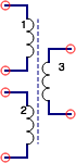
Symmetric Transformer
Symbol
Component Data
| Field | Wert |
|---|---|
| Caption | symmetrischer Transformator |
Beschreibung |
idealer symmetrischer Transformator |
| Schematic entry | sTr |
| Netlist entry | Tr |
Typ |
AnalogComponent |
| Bitmap file | symtrans |
Eigenschaften |
2 |
| Category | lumped components |
Component Parameters
| Name | Wert |
Display | Beschreibung |
|---|---|---|---|
| T1 | 1 | ja |
Spannungstransformationsverhältnis der Spule 1 |
| T2 | 1 | ja |
Spannungstransformationsverhältnis der Spule 2 |
Dc Block
Symbol

Component Data
| Field | Wert |
|---|---|
| Caption | DC-Sperre |
Beschreibung |
DC-Sperre |
| Schematic entry | DCBlock |
| Netlist entry | C |
Typ |
AnalogComponent |
| Bitmap file | dcblock |
Eigenschaften |
1 |
| Category | lumped components |
Component Parameters
| Name | Wert |
Display | Beschreibung |
|---|---|---|---|
| C | 1 uF | nein |
für die Transientensimulation: Kapazität in Farad |
Dc Feed
Symbol

Component Data
| Field | Wert |
|---|---|
| Caption | DC-Zuführung |
Beschreibung |
DC-Zuführung |
| Schematic entry | DCFeed |
| Netlist entry | L |
Typ |
AnalogComponent |
| Bitmap file | dcfeed |
Eigenschaften |
1 |
| Category | lumped components |
Component Parameters
| Name | Wert |
Display | Beschreibung |
|---|---|---|---|
| L | 1 uH | nein |
für die Transientensimulation: Induktivität in Henry |
Bias T
Symbol

Component Data
| Field | Wert |
|---|---|
| Caption | Bias T |
Beschreibung |
Bias T |
| Schematic entry | BiasT |
| Netlist entry | X |
Typ |
AnalogComponent |
| Bitmap file | biast |
Eigenschaften |
2 |
| Category | lumped components |
Component Parameters
| Name | Wert |
Display | Beschreibung |
|---|---|---|---|
| L | 1 uH | nein |
für die Transientensimulation: Induktivität in Henry |
| C | 1 uF | nein |
für die Transientensimulation: Kapazität in Farad |
Dämpfungsglied
Symbol

Component Data
| Field | Wert |
|---|---|
| Caption | Dämpfungsglied |
Beschreibung |
Dämpfungsglied |
| Schematic entry | Attenuator |
| Netlist entry | X |
Typ |
AnalogComponent |
| Bitmap file | Dämpfungsglied |
Eigenschaften |
3 |
| Category | lumped components |
Component Parameters
| Name | Wert |
Display | Beschreibung |
|---|---|---|---|
| L | 10 dB | ja |
Leistungsdämpfung |
| Zref | 50 Ohm | nein |
Referenzimpedanz |
| Temp | 26.85 | nein |
Simulationstemperatur in °C |
Verstärker
Symbol

Component Data
| Field | Wert |
|---|---|
| Caption | Verstärker |
Beschreibung |
idealer Verstärker |
| Schematic entry | Amp |
| Netlist entry | X |
Typ |
AnalogComponent |
| Bitmap file | amplifier |
Eigenschaften |
4 |
| Category | lumped components |
Component Parameters
| Name | Wert |
Display | Beschreibung |
|---|---|---|---|
| G | 10 | ja |
Spannungsverstärkung |
| Z1 | 50 Ohm | nein |
Referenzimpedanz des Eingangstors |
| Z2 | 50 Ohm | nein |
Referenzimpedanz des Ausgangstors |
| NF | 0 dB | nein |
noise figure |
Isolator
Symbol

Component Data
| Field | Wert |
|---|---|
| Caption | Isolator |
Beschreibung |
Isolator |
| Schematic entry | Isolator |
| Netlist entry | X |
Typ |
AnalogComponent |
| Bitmap file | Isolator |
Eigenschaften |
3 |
| Category | lumped components |
Component Parameters
| Name | Wert |
Display | Beschreibung |
|---|---|---|---|
| Z1 | 50 Ohm | nein |
Referenzimpedanz des Eingangstors |
| Z2 | 50 Ohm | nein |
Referenzimpedanz des Ausgangstors |
| Temp | 26.85 | nein |
Simulationstemperatur in °C |
Zirkulator
Symbol

Component Data
| Field | Wert |
|---|---|
| Caption | Zirkulator |
Beschreibung |
Zirkulator |
| Schematic entry | Circulator |
| Netlist entry | X |
Typ |
AnalogComponent |
| Bitmap file | Zirkulator |
Eigenschaften |
3 |
| Category | lumped components |
Component Parameters
| Name | Wert |
Display | Beschreibung |
|---|---|---|---|
| Z1 | 50 Ohm | nein |
Referenzimpedanz von Tor 1 |
| Z2 | 50 Ohm | nein |
Referenzimpedanz von Tor 2 |
| Z3 | 50 Ohm | nein |
Referenzimpedanz von Tor 3 |
Gyrator
Symbol

Component Data
| Field | Wert |
|---|---|
| Caption | Gyrator |
Beschreibung |
Gyrator (Impedanzinverter) |
| Schematic entry | Gyrator |
| Netlist entry | X |
Typ |
AnalogComponent |
| Bitmap file | gyrator |
Eigenschaften |
2 |
| Category | lumped components |
Component Parameters
| Name | Wert |
Display | Beschreibung |
|---|---|---|---|
| R | 50 Ohm | ja |
Gyratorverhältnis |
| Zref | 50 Ohm | nein |
Referenzimpedanz |
Phasenschieber
Symbol

Component Data
| Field | Wert |
|---|---|
| Caption | Phasenschieber |
Beschreibung |
Phasenschieber |
| Schematic entry | PShift |
| Netlist entry | X |
Typ |
AnalogComponent |
| Bitmap file | pshifter |
Eigenschaften |
2 |
| Category | lumped components |
Component Parameters
| Name | Wert |
Display | Beschreibung |
|---|---|---|---|
| phi | 90 | ja |
Phasenverschiebung in Grad |
| Zref | 50 Ohm | nein |
Referenzimpedanz |
Koppler
Symbol

Component Data
| Field | Wert |
|---|---|
| Caption | Koppler |
Beschreibung |
idealer Koppler |
| Schematic entry | Coupler |
| Netlist entry | X |
Typ |
AnalogComponent |
| Bitmap file | coupler |
Eigenschaften |
3 |
| Category | lumped components |
Component Parameters
| Name | Wert |
Display | Beschreibung |
|---|---|---|---|
| k | 0.7071 | ja |
Koppelfaktor |
| phi | 180 | ja |
Phasenverschiebung des Koppelpfades in Grad |
| Z | 50 Ohm | nein |
Referenzimpedanz |
Hybrid
Symbol

Component Data
| Field | Wert |
|---|---|
| Caption | Hybrid |
Beschreibung |
hybrid (unsymmetrical 3dB coupler) |
| Schematic entry | Hybrid |
| Netlist entry | X |
Typ |
AnalogComponent |
| Bitmap file | hybrid |
Eigenschaften |
2 |
| Category | lumped components |
Component Parameters
| Name | Wert |
Display | Beschreibung |
|---|---|---|---|
| phi | 90 | ja |
Phasenverschiebung in Grad |
| Zref | 50 Ohm | nein |
Referenzimpedanz |
Amperemeter
Symbol

Component Data
| Field | Wert |
|---|---|
| Caption | Amperemeter |
Beschreibung |
Amperemeter |
| Schematic entry | IProbe |
| Netlist entry | Pr |
Typ |
AnalogComponent |
| Bitmap file | iprobe |
Eigenschaften |
0 |
| Category | lumped components |
Voltmeter
Symbol

Component Data
| Field | Wert |
|---|---|
| Caption | Voltmeter |
Beschreibung |
Voltmeter |
| Schematic entry | VProbe |
| Netlist entry | Pr |
Typ |
AnalogComponent |
| Bitmap file | vprobe |
Eigenschaften |
0 |
| Category | lumped components |
Gekoppelte Induktivitäten
Symbol

Component Data
| Field | Wert |
|---|---|
| Caption | Gekoppelte Induktivitäten |
Beschreibung |
zwei gekoppelte Induktivitäten |
| Schematic entry | MUT |
| Netlist entry | Tr |
Typ |
AnalogComponent |
| Bitmap file | mutual |
Eigenschaften |
3 |
| Category | lumped components |
Component Parameters
| Name | Wert |
Display | Beschreibung |
|---|---|---|---|
| L1 | 1 mH | nein |
Induktivität der Spule 1 |
| L2 | 1 mH | nein |
Induktivität der Spule 2 |
| k | 0.9 | nein |
Koppelfaktor zwischen Spule 1 und 2 |
3 Gekoppelte Induktivitäten
Symbol
Component Data
| Field | Wert |
|---|---|
| Caption | 3 Gekoppelte Induktivitäten |
Beschreibung |
drei gekoppelte Induktivitäten |
| Schematic entry | MUT2 |
| Netlist entry | Tr |
Typ |
AnalogComponent |
| Bitmap file | mutual2 |
Eigenschaften |
6 |
| Category | lumped components |
Component Parameters
| Name | Wert |
Display | Beschreibung |
|---|---|---|---|
| L1 | 1 mH | nein |
Induktivität der Spule 1 |
| L2 | 1 mH | nein |
Induktivität der Spule 2 |
| L3 | 1 mH | nein |
Induktivität der Spule 3 |
| k12 | 0.9 | nein |
Koppelfaktor zwischen Spule 1 und 2 |
| k13 | 0.9 | nein |
Koppelfaktor zwischen Spule 1 und 3 |
| k23 | 0.9 | nein |
Koppelfaktor zwischen Spule 2 und 3 |
N Mutual Inductors
Symbol

Component Data
| Field | Wert |
|---|---|
| Caption | N Mutual Inductors |
Beschreibung |
several mutual inductors |
| Schematic entry | MUTX |
| Netlist entry | Tr |
Typ |
AnalogComponent |
| Bitmap file | mutualx |
Eigenschaften |
11 |
| Category | lumped components |
Component Parameters
| Name | Wert |
Display | Beschreibung |
|---|---|---|---|
| coils | 4 | nein |
number of mutual inductances |
| L1 | 1 mH | nein |
Induktivität der Spule 1 |
| L2 | 1 mH | nein |
Induktivität der Spule 2 |
| L3 | 1 mH | nein |
Induktivität der Spule 3 |
| L4 | 1 mH | nein |
inductance of coil 4 |
| k12 | 0.9 | nein |
coupling factor between coil 1 and coil 2 |
| k13 | 0.9 | nein |
coupling factor between coil 1 and coil 3 |
| k14 | 0.9 | nein |
coupling factor between coil 1 and coil 4 |
| k23 | 0.9 | nein |
coupling factor between coil 2 and coil 3 |
| k24 | 0.9 | nein |
coupling factor between coil 2 and coil 4 |
| k34 | 0.9 | nein |
coupling factor between coil 3 and coil 4 |
Switch
Symbol

Component Data
| Field | Wert |
|---|---|
| Caption | Switch |
Beschreibung |
switch (time controlled) |
| Schematic entry | Switch |
| Netlist entry | S |
Typ |
AnalogComponent |
| Bitmap file | switch |
Eigenschaften |
6 |
| Category | lumped components |
Component Parameters
| Name | Wert |
Display | Beschreibung |
|---|---|---|---|
| init | off | nein |
initial state [on, off] |
| time | 1 ms | nein |
time when state changes (semicolon separated list possible, even numbered lists are repeated) |
| Ron | 0 | nein |
Widerstand im “on”-Zustand in Ohm |
| Roff | 1e12 | nein |
Widerstand im “off”-Zustand in Ohm |
| Temp | 26.85 | nein |
Simulationstemperatur in °C |
| MaxDuration | 1e-6 | nein |
Max possible switch transition time (transition time 1/100 smallest value in ‘time’, or this number) |
Relay
Symbol

Component Data
| Field | Wert |
|---|---|
| Caption | Relay |
Beschreibung |
relay |
| Schematic entry | Relais |
| Netlist entry | S |
Typ |
AnalogComponent |
| Bitmap file | relais |
Eigenschaften |
5 |
| Category | lumped components |
Component Parameters
| Name | Wert |
Display | Beschreibung |
|---|---|---|---|
| Vt | 0.5 V | nein |
threshold voltage in Volts |
| Vh | 0.1 V | nein |
hysteresis voltage in Volts |
| Ron | 0 | nein |
resistance of “on” state in Ohms |
| Roff | 1e12 | nein |
resistance of “off” state in Ohms |
| Temp | 26.85 | nein |
Simulationstemperatur in °C |
Equation Defined Rf Device
Symbol

Component Data
| Field | Wert |
|---|---|
| Caption | Equation Defined RF Device |
Beschreibung |
equation defined RF device |
| Schematic entry | RFEDD |
| Netlist entry | RF |
Typ |
AnalogComponent |
| Bitmap file | rfedd |
Eigenschaften |
7 |
| Category | lumped components |
Component Parameters
| Name | Wert |
Display | Beschreibung |
|---|---|---|---|
Typ |
Y | nein |
type of parameters [Y, Z, S] |
| Ports | 2 | nein |
Anzahl der Tore |
| duringDC | open | nein |
representation during DC analysis [open, short, unspecified, zerofrequency] |
| P11 | 0 | nein |
parameter equation 11 |
| P12 | 0 | nein |
parameter equation 12 |
| P21 | 0 | nein |
parameter equation 21 |
| P22 | 0 | nein |
parameter equation 22 |
Equation Defined 2-Port Rf Device
Symbol
Component Data
| Field | Wert |
|---|---|
| Caption | Equation Defined 2-port RF Device |
Beschreibung |
equation defined 2-port RF device |
| Schematic entry | RFEDD2P |
| Netlist entry | RF |
Typ |
AnalogComponent |
| Bitmap file | rfedd |
Eigenschaften |
6 |
| Category | lumped components |
Component Parameters
| Name | Wert |
Display | Beschreibung |
|---|---|---|---|
Typ |
Y | nein |
type of parameters [Y, Z, S, H, G, A, T] |
| duringDC | open | nein |
representation during DC analysis [open, short, unspecified, zerofrequency] |
| P11 | 0 | nein |
parameter equation 11 |
| P12 | 0 | nein |
parameter equation 12 |
| P21 | 0 | nein |
parameter equation 21 |
| P22 | 0 | nein |
parameter equation 22 |
Sources
Dc Voltage Source
Symbol

Component Data
| Field | Wert |
|---|---|
| Caption | DC Spannungsquelle |
Beschreibung |
ideale DC Spannungsquelle |
| Schematic entry | Vdc |
| Netlist entry | V |
Typ |
AnalogComponent |
| Bitmap file | dc_voltage |
Eigenschaften |
1 |
| Category | sources |
Component Parameters
| Name | Wert |
Display | Beschreibung |
|---|---|---|---|
| U | 1 V | ja |
Spannung in Volt |
Dc Current Source
Symbol

Component Data
| Field | Wert |
|---|---|
| Caption | DC Stromquelle |
Beschreibung |
ideale DC Stromquelle |
| Schematic entry | Idc |
| Netlist entry | I |
Typ |
AnalogComponent |
| Bitmap file | dc_current |
Eigenschaften |
1 |
| Category | sources |
Component Parameters
| Name | Wert |
Display | Beschreibung |
|---|---|---|---|
| I | 1 mA | ja |
Strom in Ampere |
Ac Voltage Source
Symbol

Component Data
| Field | Wert |
|---|---|
| Caption | AC Spannungsquelle |
Beschreibung |
ideale AC Spannungsquelle |
| Schematic entry | Vac |
| Netlist entry | V |
Typ |
AnalogComponent |
| Bitmap file | ac_voltage |
Eigenschaften |
4 |
| Category | sources |
Component Parameters
| Name | Wert |
Display | Beschreibung |
|---|---|---|---|
| U | 1 V | ja |
Spitzenwert der Spannung in Volt |
| f | 1 GHz | nein |
Frequenz in Hertz |
| Phase | 0 | nein |
Anfangsphasenverschiebung in Grad |
| Theta | 0 | nein |
Dämpfungsfaktor (nur für Transientensimulation) |
Ac Current Source
Symbol

Component Data
| Field | Wert |
|---|---|
| Caption | AC Stromquelle |
Beschreibung |
ideale AC Stromquelle |
| Schematic entry | Iac |
| Netlist entry | I |
Typ |
AnalogComponent |
| Bitmap file | ac_current |
Eigenschaften |
4 |
| Category | sources |
Component Parameters
| Name | Wert |
Display | Beschreibung |
|---|---|---|---|
| I | 1 mA | ja |
Spitzenwert des Stroms in Ampere |
| f | 1 GHz | nein |
Frequenz in Hertz |
| Phase | 0 | nein |
Anfangsphasenverschiebung in Grad |
| Theta | 0 | nein |
Dämpfungsfaktor (nur für Transientensimulation) |
Signalquelle
Symbol

Component Data
| Field | Wert |
|---|---|
| Caption | Signalquelle |
Beschreibung |
AC Signalquelle |
| Schematic entry | Pac |
| Netlist entry | P |
Typ |
AnalogComponent |
| Bitmap file | source |
Eigenschaften |
5 |
| Category | sources |
Component Parameters
| Name | Wert |
Display | Beschreibung |
|---|---|---|---|
| Num | 1 | ja |
Tornummer |
| Z | 50 Ohm | ja |
Torimpedanz |
| P | 0 dBm | nein |
(available) ac power in Watts |
| f | 1 GHz | nein |
Frequenz in Hertz |
| Temp | 26.85 | nein |
Simulationstemperatur in °C |
Rauschspannungsquelle
Symbol

Component Data
| Field | Wert |
|---|---|
| Caption | Rauschspannungsquelle |
Beschreibung |
Rauschspannungsquelle |
| Schematic entry | Vnoise |
| Netlist entry | V |
Typ |
AnalogComponent |
| Bitmap file | noise_volt |
Eigenschaften |
4 |
| Category | sources |
Component Parameters
| Name | Wert |
Display | Beschreibung |
|---|---|---|---|
| u | 1e-6 | ja |
spektrale Rauschspannungsleistungsdichte in V²/Hz |
| e | 0 | nein |
Frequenzexponent |
| c | 1 | nein |
Frequenzkoeffizient |
| a | 0 | nein |
additiver Frequenzterm |
Rauschstromquelle
Symbol

Component Data
| Field | Wert |
|---|---|
| Caption | Rauschstromquelle |
Beschreibung |
Rauschstromquelle |
| Schematic entry | Inoise |
| Netlist entry | I |
Typ |
AnalogComponent |
| Bitmap file | noise_current |
Eigenschaften |
4 |
| Category | sources |
Component Parameters
| Name | Wert |
Display | Beschreibung |
|---|---|---|---|
| i | 1e-6 | ja |
spektrale Rauschstromleistungsdichte in A²/Hz |
| e | 0 | nein |
Frequenzexponent |
| c | 1 | nein |
Frequenzkoeffizient |
| a | 0 | nein |
additiver Frequenzterm |
spannungsgesteuerte Stromquelle
Symbol

Component Data
| Field | Wert |
|---|---|
| Caption | spannungsgesteuerte Stromquelle |
Beschreibung |
spannungsgesteuerte Stromquelle |
| Schematic entry | VCCS |
| Netlist entry | SRC |
Typ |
AnalogComponent |
| Bitmap file | vccs |
Eigenschaften |
2 |
| Category | sources |
Component Parameters
| Name | Wert |
Display | Beschreibung |
|---|---|---|---|
| G | 1 S | ja |
Vorwärtstranskonduktanz |
| T | 0 | nein |
Verzögerungszeit |
stromgesteuerte Stromquelle
Symbol

Component Data
| Field | Wert |
|---|---|
| Caption | stromgesteuerte Stromquelle |
Beschreibung |
stromgesteuerte Stromquelle |
| Schematic entry | CCCS |
| Netlist entry | SRC |
Typ |
AnalogComponent |
| Bitmap file | cccs |
Eigenschaften |
2 |
| Category | sources |
Component Parameters
| Name | Wert |
Display | Beschreibung |
|---|---|---|---|
| G | 1 | ja |
Vorwärtstransferfaktor |
| T | 0 | nein |
Verzögerungszeit |
spannungsgesteuerte Spannungsquelle
Symbol

Component Data
| Field | Wert |
|---|---|
| Caption | spannungsgesteuerte Spannungsquelle |
Beschreibung |
spannungsgesteuerte Spannungsquelle |
| Schematic entry | VCVS |
| Netlist entry | SRC |
Typ |
AnalogComponent |
| Bitmap file | vcvs |
Eigenschaften |
2 |
| Category | sources |
Component Parameters
| Name | Wert |
Display | Beschreibung |
|---|---|---|---|
| G | 1 | ja |
Vorwärtstransferfaktor |
| T | 0 | nein |
Verzögerungszeit |
stromgesteuerte Spannungsquelle
Symbol

Component Data
| Field | Wert |
|---|---|
| Caption | stromgesteuerte Spannungsquelle |
Beschreibung |
stromgesteuerte Spannungsquelle |
| Schematic entry | CCVS |
| Netlist entry | SRC |
Typ |
AnalogComponent |
| Bitmap file | ccvs |
Eigenschaften |
2 |
| Category | sources |
Component Parameters
| Name | Wert |
Display | Beschreibung |
|---|---|---|---|
| G | 1 Ohm | ja |
Vorwärtstransferfaktor |
| T | 0 | nein |
Verzögerungszeit |
Spannungspulsquelle
Symbol

Component Data
| Field | Wert |
|---|---|
| Caption | Spannungspulsquelle |
Beschreibung |
ideale Spannungspulsquelle |
| Schematic entry | Vpulse |
| Netlist entry | V |
Typ |
AnalogComponent |
| Bitmap file | vpulse |
Eigenschaften |
6 |
| Category | sources |
Component Parameters
| Name | Wert |
Display | Beschreibung |
|---|---|---|---|
| U1 | 0 V | ja |
Spannung vor und nach dem Puls |
| U2 | 1 V | ja |
Spannung während des Pulses |
| T1 | 0 | ja |
Anfangszeit des Pulses |
| T2 | 1 ms | ja |
Endzeit des Pulses |
| Tr | 1 ns | nein |
Anstiegszeit des Pulses |
| Tf | 1 ns | nein |
Abfallszeit des Pulses |
Strompulsquelle
Symbol

Component Data
| Field | Wert |
|---|---|
| Caption | Strompulsquelle |
Beschreibung |
ideale Pulsstromquelle |
| Schematic entry | Ipulse |
| Netlist entry | I |
Typ |
AnalogComponent |
| Bitmap file | ipulse |
Eigenschaften |
6 |
| Category | sources |
Component Parameters
| Name | Wert |
Display | Beschreibung |
|---|---|---|---|
| I1 | 0 | ja |
Strom vor und nach dem Puls |
| I2 | 1 A | ja |
Strom während des Pulses |
| T1 | 0 | ja |
Anfangszeit des Pulses |
| T2 | 1 ms | ja |
Endzeit des Pulses |
| Tr | 1 ns | nein |
Anstiegszeit des Pulses |
| Tf | 1 ns | nein |
Abfallszeit des Pulses |
Rechteckspannungsquelle
Symbol

Component Data
| Field | Wert |
|---|---|
| Caption | Rechteckspannungsquelle |
Beschreibung |
ideale Rechteckspannungsquelle |
| Schematic entry | Vrect |
| Netlist entry | V |
Typ |
AnalogComponent |
| Bitmap file | vrect |
Eigenschaften |
6 |
| Category | sources |
Component Parameters
| Name | Wert |
Display | Beschreibung |
|---|---|---|---|
| U | 1 V | ja |
Spannung der High-Level Pulse |
| TH | 1 ms | ja |
Dauer der High-Level Pulse |
| TL | 1 ms | ja |
Dauer der Low-Level Pulse |
| Tr | 1 ns | nein |
Anstiegszeit des Pulses |
| Tf | 1 ns | nein |
Abfallszeit des Pulses |
| Td | 0 ns | nein |
initial delay time |
Rechteckstromquelle
Symbol

Component Data
| Field | Wert |
|---|---|
| Caption | Rechteckstromquelle |
Beschreibung |
ideale Rechteckstromquelle |
| Schematic entry | Irect |
| Netlist entry | I |
Typ |
AnalogComponent |
| Bitmap file | irect |
Eigenschaften |
6 |
| Category | sources |
Component Parameters
| Name | Wert |
Display | Beschreibung |
|---|---|---|---|
| I | 1 mA | ja |
Strom während des Rechteckpulses |
| TH | 1 ms | ja |
Dauer der High-Level Pulse |
| TL | 1 ms | ja |
Dauer der Low-Level Pulse |
| Tr | 1 ns | nein |
Anstiegszeit des Pulses |
| Tf | 1 ns | nein |
Abfallszeit des Pulses |
| Td | 0 ns | nein |
initial delay time |
Korrelierte Rauschquellen
Symbol

Component Data
| Field | Wert |
|---|---|
| Caption | Korrelierte Rauschquellen |
Beschreibung |
korrelierte Stromquellen |
| Schematic entry | IInoise |
| Netlist entry | SRC |
Typ |
AnalogComponent |
| Bitmap file | noise_ii |
Eigenschaften |
6 |
| Category | sources |
Component Parameters
| Name | Wert |
Display | Beschreibung |
|---|---|---|---|
| i1 | 1e-6 | ja |
spektrale Rauschstromleistungsdichte der Quelle 1 |
| i2 | 1e-6 | ja |
spektrale Rauschstromleistungsdichte der Quelle 2 |
| C | 0.5 | ja |
normierter Korrelationskoeffizient |
| e | 0 | nein |
Frequenzexponent |
| c | 1 | nein |
Frequenzkoeffizient |
| a | 0 | nein |
additiver Frequenzterm |
Korrelierte Rauschquellen
Symbol

Component Data
| Field | Wert |
|---|---|
| Caption | Korrelierte Rauschquellen |
Beschreibung |
korrelierte Stromquellen |
| Schematic entry | VVnoise |
| Netlist entry | SRC |
Typ |
AnalogComponent |
| Bitmap file | noise_vv |
Eigenschaften |
6 |
| Category | sources |
Component Parameters
| Name | Wert |
Display | Beschreibung |
|---|---|---|---|
| v1 | 1e-6 | ja |
spektrale Rauschspannungsleistungsdichte der Quelle 1 |
| v2 | 1e-6 | ja |
spektrale Rauschspannungsleistungsdichte der Quelle 2 |
| C | 0.5 | ja |
normierter Korrelationskoeffizient |
| e | 0 | nein |
Frequenzexponent |
| c | 1 | nein |
Frequenzkoeffizient |
| a | 0 | nein |
additiver Frequenzterm |
Korrelierte Rauschquellen
Symbol

Component Data
| Field | Wert |
|---|---|
| Caption | Korrelierte Rauschquellen |
Beschreibung |
korrelierte Stromquellen |
| Schematic entry | IVnoise |
| Netlist entry | SRC |
Typ |
AnalogComponent |
| Bitmap file | noise_iv |
Eigenschaften |
6 |
| Category | sources |
Component Parameters
| Name | Wert |
Display | Beschreibung |
|---|---|---|---|
| i1 | 1e-6 | ja |
spektrale Rauschstromleistungsdichte der Quelle 1 |
| v2 | 1e-6 | ja |
spektrale Rauschspannungsleistungsdichte der Quelle 2 |
| C | 0.5 | ja |
normierter Korrelationskoeffizient |
| e | 0 | nein |
Frequenzexponent |
| c | 1 | nein |
Frequenzkoeffizient |
| a | 0 | nein |
additiver Frequenzterm |
Am Modulated Source
Symbol

Component Data
| Field | Wert |
|---|---|
| Caption | AM modulierte Quelle |
Beschreibung |
AC-Spannungsquelle mit Amplitudenmodulator |
| Schematic entry | AM_Mod |
| Netlist entry | V |
Typ |
AnalogComponent |
| Bitmap file | am_mod |
Eigenschaften |
4 |
| Category | sources |
Component Parameters
| Name | Wert |
Display | Beschreibung |
|---|---|---|---|
| U | 1 V | ja |
Spitzenwert der Spannung in Volt |
| f | 1 GHz | nein |
Frequenz in Hertz |
| Phase | 0 | nein |
Anfangsphasenverschiebung in Grad |
| m | 1.0 | nein |
Modulationsindex |
Pm Modulated Source
Symbol

Component Data
| Field | Wert |
|---|---|
| Caption | PM modulierte Quelle |
Beschreibung |
AC-Spannungsquelle mit Phasenmodulator |
| Schematic entry | PM_Mod |
| Netlist entry | V |
Typ |
AnalogComponent |
| Bitmap file | pm_mod |
Eigenschaften |
4 |
| Category | sources |
Component Parameters
| Name | Wert |
Display | Beschreibung |
|---|---|---|---|
| U | 1 V | ja |
Spitzenwert der Spannung in Volt |
| f | 1 GHz | nein |
Frequenz in Hertz |
| Phase | 0 | nein |
Anfangsphasenverschiebung in Grad |
| M | 1.0 | nein |
Modulationsindex |
Exponential Current Pulse
Symbol

Component Data
| Field | Wert |
|---|---|
| Caption | Exponential Current Pulse |
Beschreibung |
exponential current source |
| Schematic entry | Iexp |
| Netlist entry | I |
Typ |
AnalogComponent |
| Bitmap file | iexp |
Eigenschaften |
6 |
| Category | sources |
Component Parameters
| Name | Wert |
Display | Beschreibung |
|---|---|---|---|
| I1 | 0 | ja |
current before rising edge |
| I2 | 1 A | ja |
maximum current of the pulse |
| T1 | 0 | ja |
start time of the exponentially rising edge |
| T2 | 1 ms | ja |
start of exponential decay |
| Tr | 1 ns | nein |
time constant of the rising edge |
| Tf | 1 ns | nein |
time constant of the falling edge |
Exponential Voltage Pulse
Symbol

Component Data
| Field | Wert |
|---|---|
| Caption | Exponential Voltage Pulse |
Beschreibung |
exponential voltage source |
| Schematic entry | Vexp |
| Netlist entry | V |
Typ |
AnalogComponent |
| Bitmap file | vexp |
Eigenschaften |
6 |
| Category | sources |
Component Parameters
| Name | Wert |
Display | Beschreibung |
|---|---|---|---|
| U1 | 0 V | ja |
voltage before rising edge |
| U2 | 1 V | ja |
maximum voltage of the pulse |
| T1 | 0 | ja |
start time of the exponentially rising edge |
| T2 | 1 ms | ja |
start of exponential decay |
| Tr | 1 ns | nein |
rise time of the rising edge |
| Tf | 1 ns | nein |
fall time of the falling edge |
File Based Voltage Source
Symbol

Component Data
| Field | Wert |
|---|---|
| Caption | File Based Voltage Source |
Beschreibung |
file based voltage source |
| Schematic entry | Vfile |
| Netlist entry | V |
Typ |
AnalogComponent |
| Bitmap file | vfile |
Eigenschaften |
5 |
| Category | sources |
Component Parameters
| Name | Wert |
Display | Beschreibung |
|---|---|---|---|
Datei |
vfile.dat | ja |
name of the sample file |
| Interpolator | linear | nein |
interpolation type [hold, linear, cubic] |
| Repeat | nein |
nein |
repeat waveform [no, yes] |
| G | 1 | nein |
Spannungsverstärkung |
| T | 0 | nein |
Verzögerungszeit |
File Based Current Source
Symbol

Component Data
| Field | Wert |
|---|---|
| Caption | File Based Current Source |
Beschreibung |
file based current source |
| Schematic entry | Ifile |
| Netlist entry | I |
Typ |
AnalogComponent |
| Bitmap file | ifile |
Eigenschaften |
5 |
| Category | sources |
Component Parameters
| Name | Wert |
Display | Beschreibung |
|---|---|---|---|
Datei |
ifile.dat | ja |
name of the sample file |
| Interpolator | linear | nein |
interpolation type [hold, linear, cubic] |
| Repeat | nein |
nein |
repeat waveform [no, yes] |
| G | 1 | nein |
current gain |
| T | 0 | nein |
Verzögerungszeit |
Probes
Transmission Lines
Übertragungsstrecke
Symbol

Component Data
| Field | Wert |
|---|---|
| Caption | Übertragungsstrecke |
Beschreibung |
ideale Leitung |
| Schematic entry | TLIN |
| Netlist entry | Line |
Typ |
AnalogComponent |
| Bitmap file | tline |
Eigenschaften |
4 |
| Category | transmission lines |
Component Parameters
| Name | Wert |
Display | Beschreibung |
|---|---|---|---|
| Z | 50 Ohm | ja |
charakteristische Impedanz |
| L | 1 mm | ja |
elektrische Länge der Leitung |
| Alpha | 0 dB | nein |
attenuation factor per length in 1/m |
| Temp | 26.85 | nein |
Simulationstemperatur in °C |
4-Terminal Transmission Line
Symbol

Component Data
| Field | Wert |
|---|---|
| Caption | 4-Terminal Transmission Line |
Beschreibung |
ideal 4-terminal transmission line |
| Schematic entry | TLIN4P |
| Netlist entry | Line |
Typ |
AnalogComponent |
| Bitmap file | tline_4port |
Eigenschaften |
4 |
| Category | transmission lines |
Component Parameters
| Name | Wert |
Display | Beschreibung |
|---|---|---|---|
| Z | 50 Ohm | ja |
charakteristische Impedanz |
| L | 1 mm | ja |
elektrische Länge der Leitung |
| Alpha | 0 dB | nein |
attenuation factor per length in 1/m |
| Temp | 26.85 | nein |
Simulationstemperatur in °C |
Coupled Transmission Line
Symbol

Component Data
| Field | Wert |
|---|---|
| Caption | Coupled Transmission Line |
Beschreibung |
coupled transmission lines |
| Schematic entry | CTLIN |
| Netlist entry | Line |
Typ |
AnalogComponent |
| Bitmap file | ctline |
Eigenschaften |
8 |
| Category | transmission lines |
Component Parameters
| Name | Wert |
Display | Beschreibung |
|---|---|---|---|
| Ze | 50 Ohm | ja |
characteristic impedance of even mode |
| Zo | 50 Ohm | ja |
characteristic impedance of odd mode |
| L | 1 mm | ja |
elektrische Länge der Leitung |
| Ere | 1 | nein |
relative dielectric constant of even mode |
| Ero | 1 | nein |
relative dielectric constant of odd mode |
| Ae | 0 dB | nein |
attenuation factor per length of even mode |
| Ao | 0 dB | nein |
attenuation factor per length of odd mode |
| Temp | 26.85 | nein |
Simulationstemperatur in °C |
Twisted-Pair
Symbol

Component Data
| Field | Wert |
|---|---|
| Caption | Twisted-Pair |
Beschreibung |
twisted pair transmission line |
| Schematic entry | TWIST |
| Netlist entry | Line |
Typ |
AnalogComponent |
| Bitmap file | twistedpair |
Eigenschaften |
9 |
| Category | transmission lines |
Component Parameters
| Name | Wert |
Display | Beschreibung |
|---|---|---|---|
| d | 0.5 mm | ja |
diameter of conductor |
| D | 0.8 mm | ja |
diameter of wire (conductor and insulator) |
| L | 1.5 | ja |
physical length of the line |
| T | 100 | nein |
twists per length in 1/m |
| er | 4 | nein |
dielectric constant of insulator |
| mur | 1 | nein |
relative Permeabilität des Leiters |
| rho | 0.022e-6 | nein |
spezifischer Widerstand des Leiters |
| tand | 4e-4 | nein |
dielektrischer Verlustwinkel |
| Temp | 26.85 | nein |
Simulationstemperatur in °C |
Koaxialkabel
Symbol

Component Data
| Field | Wert |
|---|---|
| Caption | Koaxialkabel |
Beschreibung |
Koaxialleitung |
| Schematic entry | COAX |
| Netlist entry | Line |
Typ |
AnalogComponent |
| Bitmap file | coaxial |
Eigenschaften |
8 |
| Category | transmission lines |
Component Parameters
| Name | Wert |
Display | Beschreibung |
|---|---|---|---|
| er | 2.29 | ja |
relative Permittivität des Dielektrikums |
| rho | 0.022e-6 | nein |
spezifischer Widerstand des Leiters |
| mur | 1 | nein |
relative Permeabilität des Leiters |
| D | 2.95 mm | nein |
innerer Durchmesser des Außenleiters |
| d | 0.9 mm | nein |
Durchmesser des Innenleiters |
| L | 1500 mm | ja |
mechanische Länge der Leitung |
| tand | 4e-4 | nein |
dielektrischer Verlustwinkel |
| Temp | 26.85 | nein |
Simulationstemperatur in °C |
Rectangular Waveguide
Symbol

Component Data
| Field | Wert |
|---|---|
| Caption | Rectangular Waveguide |
Beschreibung |
Rectangular Waveguide |
| Schematic entry | RECTLINE |
| Netlist entry | Line |
Typ |
AnalogComponent |
| Bitmap file | rectline |
Eigenschaften |
9 |
| Category | transmission lines |
Component Parameters
| Name | Wert |
Display | Beschreibung |
|---|---|---|---|
| a | 2.95 mm | ja |
widest side |
| b | 0.9 mm | ja |
shortest side |
| L | 1500 mm | ja |
mechanische Länge der Leitung |
| er | 1 | nein |
relative Permittivität des Dielektrikums |
| mur | 1 | nein |
relative Permeabilität des Leiters |
| tand | 0 | nein |
dielektrischer Verlustwinkel |
| rho | 0.022e-6 | nein |
spezifischer Widerstand des Leiters |
| Temp | 26.85 | nein |
Simulationstemperatur in °C |
| Material | unspecified | nein |
material parameter for temperature model [unspecified, Copper, StainlessSteel, Gold] |
Rlcg Transmission Line
Symbol

Component Data
| Field | Wert |
|---|---|
| Caption | RLCG Transmission Line |
Beschreibung |
RLCG transmission line |
| Schematic entry | RLCG |
| Netlist entry | Line |
Typ |
AnalogComponent |
| Bitmap file | rlcg |
Eigenschaften |
6 |
| Category | transmission lines |
Component Parameters
| Name | Wert |
Display | Beschreibung |
|---|---|---|---|
| R | 0.0 | nein |
resistive load (Ohm/m) |
| L | 0.6e-6 | ja |
inductive load (H/m) |
| C | 240e-12 | ja |
capacitive load (F/m) |
| G | 0.0 | nein |
conductive load (S/m) |
Länge |
1 mm | ja |
elektrische Länge der Leitung |
| Temp | 26.85 | nein |
Simulationstemperatur in °C |
Substrat
Symbol

Component Data
| Field | Wert |
|---|---|
| Caption | Substrat |
Beschreibung |
Substratdefinition |
| Schematic entry | SUBST |
| Netlist entry | Subst |
Typ |
AnalogComponent |
| Bitmap file | Substrat |
Eigenschaften |
6 |
| Category | transmission lines |
Component Parameters
| Name | Wert |
Display | Beschreibung |
|---|---|---|---|
| er | 9.8 | ja |
relative Permeabilität |
| h | 1 mm | ja |
Höhe in Metern |
| t | 35 um | ja |
Metallisierungsdicke |
| tand | 2e-4 | ja |
dielektrischer Verlustwinkel |
| rho | 0.022e-6 | ja |
spezifischer Widerstand des Metalls |
| D | 0.15e-6 | ja |
effektive Oberflächenrauhtiefe |
Mikrostreifenleitung
Symbol

Component Data
| Field | Wert |
|---|---|
| Caption | Mikrostreifenleitung |
Beschreibung |
Mikrostreifenleitung |
| Schematic entry | MLIN |
| Netlist entry | MS |
Typ |
AnalogComponent |
| Bitmap file | msline |
Eigenschaften |
6 |
| Category | transmission lines |
Component Parameters
| Name | Wert |
Display | Beschreibung |
|---|---|---|---|
| Subst | Subst1 | ja |
Name der Substratdefinition |
| W | 1 mm | ja |
Leitungsbreite |
| L | 10 mm | ja |
Leitungslänge |
| Model | Hammerstad | nein |
quasi-static microstrip model [Hammerstad, Wheeler, Schneider] |
| DispModel | Kirschning | nein |
microstrip dispersion model [Kirschning, Kobayashi, Yamashita, Hammerstad, Getsinger, Schneider, Pramanick] |
| Temp | 26.85 | nein |
Simulationstemperatur in °C |
gekoppelte Mikrostreifenleitung
Symbol

Component Data
| Field | Wert |
|---|---|
| Caption | gekoppelte Mikrostreifenleitung |
Beschreibung |
gekoppelte Mikrostreifenleitung |
| Schematic entry | MCOUPLED |
| Netlist entry | MS |
Typ |
AnalogComponent |
| Bitmap file | mscoupled |
Eigenschaften |
7 |
| Category | transmission lines |
Component Parameters
| Name | Wert |
Display | Beschreibung |
|---|---|---|---|
| Subst | Subst1 | ja |
Name der Substratdefinition |
| W | 1 mm | ja |
Leitungsbreite |
| L | 10 mm | ja |
Leitungslänge |
| S | 1 mm | ja |
Abstand zwischen den Leitungen |
| Model | Kirschning | nein |
microstrip model [Kirschning, Hammerstad] |
| DispModel | Kirschning | nein |
microstrip dispersion model [Kirschning, Getsinger] |
| Temp | 26.85 | nein |
Simulationstemperatur in °C |
Microstrip Lange Coupler
Symbol

Component Data
| Field | Wert |
|---|---|
| Caption | Microstrip Lange Coupler |
Beschreibung |
microstrip lange coupler |
| Schematic entry | MLANGE |
| Netlist entry | MS |
Typ |
AnalogComponent |
| Bitmap file | mslange |
Eigenschaften |
7 |
| Category | transmission lines |
Component Parameters
| Name | Wert |
Display | Beschreibung |
|---|---|---|---|
| Subst | Subst1 | ja |
Name der Substratdefinition |
| W | 1 mm | ja |
Leitungsbreite |
| L | 10 mm | ja |
Leitungslänge |
| S | 1 mm | ja |
Abstand zwischen den Leitungen |
| Model | Kirschning | nein |
microstrip model [Kirschning, Hammerstad] |
| DispModel | Kirschning | nein |
microstrip dispersion model [Kirschning, Getsinger] |
| Temp | 26.85 | nein |
Simulationstemperatur in °C |
Mikrostreifenwinkel
Symbol

Component Data
| Field | Wert |
|---|---|
| Caption | Mikrostreifenwinkel |
Beschreibung |
Mikrostreifenwinkel |
| Schematic entry | MCORN |
| Netlist entry | MS |
Typ |
AnalogComponent |
| Bitmap file | mscorner |
Eigenschaften |
2 |
| Category | transmission lines |
Component Parameters
| Name | Wert |
Display | Beschreibung |
|---|---|---|---|
| Subst | Subst1 | ja |
Substrat |
| W | 1 mm | ja |
Streifenbreite |
Abgeflachter Mikrostreifenwinkel
Symbol

Component Data
| Field | Wert |
|---|---|
| Caption | Abgeflachter Mikrostreifenwinkel |
Beschreibung |
abgeflachter Mikrostreifenwinkel |
| Schematic entry | MMBEND |
| Netlist entry | MS |
Typ |
AnalogComponent |
| Bitmap file | msmbend |
Eigenschaften |
2 |
| Category | transmission lines |
Component Parameters
| Name | Wert |
Display | Beschreibung |
|---|---|---|---|
| Subst | Subst1 | ja |
Substrat |
| W | 1 mm | ja |
Streifenbreite |
Mikrostreifenabsatz
Symbol

Component Data
| Field | Wert |
|---|---|
| Caption | Mikrostreifenabsatz |
Beschreibung |
Mikrostreifenabsatz |
| Schematic entry | MSTEP |
| Netlist entry | MS |
Typ |
AnalogComponent |
| Bitmap file | msstep |
Eigenschaften |
5 |
| Category | transmission lines |
Component Parameters
| Name | Wert |
Display | Beschreibung |
|---|---|---|---|
| Subst | Subst1 | ja |
Substrat |
| W1 | 2 mm | ja |
Breite der Leitung 1 |
| W2 | 1 mm | ja |
Breite der Leitung 2 |
| MSModel | Hammerstad | nein |
quasi-static microstrip model [Hammerstad, Wheeler, Schneider] |
| MSDispModel | Kirschning | nein |
microstrip dispersion model [Kirschning, Kobayashi, Yamashita, Hammerstad, Getsinger, Schneider, Pramanick] |
Mikrostreifen T-Verzweigung
Symbol

Component Data
| Field | Wert |
|---|---|
| Caption | Mikrostreifen T-Verzweigung |
Beschreibung |
T-Verzweigung einer Mikrostreifenleitung |
| Schematic entry | MTEE |
| Netlist entry | MS |
Typ |
AnalogComponent |
| Bitmap file | mstee |
Eigenschaften |
8 |
| Category | transmission lines |
Component Parameters
| Name | Wert |
Display | Beschreibung |
|---|---|---|---|
| Subst | Subst1 | ja |
Substrat |
| W1 | 1 mm | ja |
Leitungsbreite 1 |
| W2 | 1 mm | ja |
Leitungsbreite 2 |
| W3 | 2 mm | ja |
Leitungsbreite 3 |
| MSModel | Hammerstad | nein |
quasi-static microstrip model [Hammerstad, Wheeler, Schneider] |
| MSDispModel | Kirschning | nein |
microstrip dispersion model [Kirschning, Kobayashi, Yamashita, Hammerstad, Getsinger, Schneider, Pramanick] |
| Temp | 26.85 | nein |
Temperatur in °C |
| Symbol | showNumbers | nein |
show port numbers in symbol or not [showNumbers, noNumbers] |
Mikrostreifenkreuzung
Symbol

Component Data
| Field | Wert |
|---|---|
| Caption | Mikrostreifenkreuzung |
Beschreibung |
Mikrostreifenkreuzung |
| Schematic entry | MCROSS |
| Netlist entry | MS |
Typ |
AnalogComponent |
| Bitmap file | mscross |
Eigenschaften |
8 |
| Category | transmission lines |
Component Parameters
| Name | Wert |
Display | Beschreibung |
|---|---|---|---|
| Subst | Subst1 | ja |
Substrat |
| W1 | 1 mm | ja |
Leitungsbreite 1 |
| W2 | 2 mm | ja |
Leitungsbreite 2 |
| W3 | 1 mm | ja |
Leitungsbreite 3 |
| W4 | 2 mm | ja |
Leitungsbreite 4 |
| MSModel | Hammerstad | nein |
quasi-static microstrip model [Hammerstad, Wheeler, Schneider] |
| MSDispModel | Kirschning | nein |
microstrip dispersion model [Kirschning, Kobayashi, Yamashita, Hammerstad, Getsinger, Schneider, Pramanick] |
| Symbol | showNumbers | nein |
show port numbers in symbol or not [showNumbers, noNumbers] |
Offene Mikrostreifenleitung
Symbol

Component Data
| Field | Wert |
|---|---|
| Caption | Offene Mikrostreifenleitung |
Beschreibung |
offenen Mikrostreifenleitung |
| Schematic entry | MOPEN |
| Netlist entry | MS |
Typ |
AnalogComponent |
| Bitmap file | msopen |
Eigenschaften |
5 |
| Category | transmission lines |
Component Parameters
| Name | Wert |
Display | Beschreibung |
|---|---|---|---|
| Subst | Subst1 | ja |
Name der Substratdefinition |
| W | 1 mm | ja |
Leitungsbreite |
| MSModel | Hammerstad | nein |
quasi-static microstrip model [Hammerstad, Wheeler, Schneider] |
| MSDispModel | Kirschning | nein |
microstrip dispersion model [Kirschning, Kobayashi, Yamashita, Hammerstad, Getsinger, Schneider, Pramanick] |
| Model | Kirschning | nein |
microstrip open end model [Kirschning, Hammerstad, Alexopoulos] |
Mikrostreifenlücke
Symbol

Component Data
| Field | Wert |
|---|---|
| Caption | Mikrostreifenlücke |
Beschreibung |
Mikrostreifenlücke |
| Schematic entry | MGAP |
| Netlist entry | MS |
Typ |
AnalogComponent |
| Bitmap file | msgap |
Eigenschaften |
6 |
| Category | transmission lines |
Component Parameters
| Name | Wert |
Display | Beschreibung |
|---|---|---|---|
| Subst | Subst1 | ja |
Name der Substratdefinition |
| W1 | 1 mm | ja |
Breite der Leitung 1 |
| W2 | 1 mm | ja |
Breite der Leitung 2 |
| S | 1 mm | ja |
Abstand zwischen den Mikrostreifenenden |
| MSModel | Hammerstad | nein |
quasi-static microstrip model [Hammerstad, Wheeler, Schneider] |
| MSDispModel | Kirschning | nein |
microstrip dispersion model [Kirschning, Kobayashi, Yamashita, Hammerstad, Getsinger, Schneider, Pramanick] |
Mikrostreifendurchkontaktierung
Symbol

Component Data
| Field | Wert |
|---|---|
| Caption | Mikrostreifendurchkontaktierung |
Beschreibung |
Mikrostreifendurchkontaktierung |
| Schematic entry | MVIA |
| Netlist entry | MS |
Typ |
AnalogComponent |
| Bitmap file | msvia |
Eigenschaften |
3 |
| Category | transmission lines |
Component Parameters
| Name | Wert |
Display | Beschreibung |
|---|---|---|---|
| Subst | Subst1 | ja |
Substrat |
| D | 1 mm | ja |
Durchmesser der runden Durchkontaktierung |
| Temp | 26.85 | nein |
Simulationstemperatur in °C |
Microstrip Radial Stub
Symbol

Component Data
| Field | Wert |
|---|---|
| Caption | Microstrip Radial Stub |
Beschreibung |
microstrip radial stub |
| Schematic entry | MRSTUB |
| Netlist entry | MS |
Typ |
AnalogComponent |
| Bitmap file | msrstub |
Eigenschaften |
4 |
| Category | transmission lines |
Component Parameters
| Name | Wert |
Display | Beschreibung |
|---|---|---|---|
| Subst | Subst1 | ja |
Name der Substratdefinition |
| ri | 1 mm | nein |
inner radius |
| ro | 10 mm | ja |
outer radius |
| alpha | 90 | ja |
stub angle (degrees) |
Koplanarleitung
Symbol

Component Data
| Field | Wert |
|---|---|
| Caption | Koplanarleitung |
Beschreibung |
Koplanarleitung |
| Schematic entry | CLIN |
| Netlist entry | CL |
Typ |
AnalogComponent |
| Bitmap file | coplanar |
Eigenschaften |
6 |
| Category | transmission lines |
Component Parameters
| Name | Wert |
Display | Beschreibung |
|---|---|---|---|
| Subst | Subst1 | ja |
Name der Substratdefinition |
| W | 1 mm | ja |
Leitungsbreite |
| S | 1 mm | ja |
Schlitzbreite |
| L | 10 mm | ja |
Leitungslänge |
| Backside | Air | nein |
material at the backside of the substrate [Metal, Air] |
| Approx | ja |
nein |
use approximation instead of precise equation [yes, no] |
Offene Koplanarleitung
Symbol

Component Data
| Field | Wert |
|---|---|
| Caption | Offene Koplanarleitung |
Beschreibung |
offene Koplanarleitung |
| Schematic entry | COPEN |
| Netlist entry | CL |
Typ |
AnalogComponent |
| Bitmap file | cpwopen |
Eigenschaften |
5 |
| Category | transmission lines |
Component Parameters
| Name | Wert |
Display | Beschreibung |
|---|---|---|---|
| Subst | Subst1 | ja |
Name der Substratdefinition |
| W | 1 mm | ja |
Leitungsbreite |
| S | 1 mm | ja |
Schlitzbreite |
| G | 5 mm | ja |
Spaltbreite am Ende der Leitung |
| Backside | Air | nein |
material at the backside of the substrate [Metal, Air] |
Kurzgeschlossene Koplanarleitung
Symbol

Component Data
| Field | Wert |
|---|---|
| Caption | Kurzgeschlossene Koplanarleitung |
Beschreibung |
kurzgeschlossene Koplanarleitung |
| Schematic entry | CSHORT |
| Netlist entry | CL |
Typ |
AnalogComponent |
| Bitmap file | cpwshort |
Eigenschaften |
4 |
| Category | transmission lines |
Component Parameters
| Name | Wert |
Display | Beschreibung |
|---|---|---|---|
| Subst | Subst1 | ja |
Name der Substratdefinition |
| W | 1 mm | ja |
Leitungsbreite |
| S | 1 mm | ja |
Schlitzbreite |
| Backside | Air | nein |
material at the backside of the substrate [Metal, Air] |
Koplanarlücke
Symbol

Component Data
| Field | Wert |
|---|---|
| Caption | Koplanarlücke |
Beschreibung |
Koplanarlücke |
| Schematic entry | CGAP |
| Netlist entry | CL |
Typ |
AnalogComponent |
| Bitmap file | cpwgap |
Eigenschaften |
4 |
| Category | transmission lines |
Component Parameters
| Name | Wert |
Display | Beschreibung |
|---|---|---|---|
| Subst | Subst1 | ja |
Name der Substratdefinition |
| W | 1 mm | ja |
Leitungsbreite |
| S | 1 mm | ja |
Schlitzbreite |
| G | 0.5 mm | ja |
Abstand zwischen den Koplanarleitungsenden |
Koplanarabsatz
Symbol

Component Data
| Field | Wert |
|---|---|
| Caption | Koplanarabsatz |
Beschreibung |
Koplanarabsatz |
| Schematic entry | CSTEP |
| Netlist entry | CL |
Typ |
AnalogComponent |
| Bitmap file | cpwstep |
Eigenschaften |
5 |
| Category | transmission lines |
Component Parameters
| Name | Wert |
Display | Beschreibung |
|---|---|---|---|
| Subst | Subst1 | ja |
Name der Substratdefinition |
| W1 | 1 mm | ja |
Leitungsbreite 1 |
| W2 | 2 mm | ja |
Leitungsbreite 2 |
| S | 3 mm | ja |
Abstand zwischen den Masseebenen |
| Backside | Air | nein |
material at the backside of the substrate [Metal, Air] |
Bond Wire
Symbol

Component Data
| Field | Wert |
|---|---|
| Caption | Bond Wire |
Beschreibung |
bond wire |
| Schematic entry | BOND |
| Netlist entry | Line |
Typ |
AnalogComponent |
| Bitmap file | bondwire |
Eigenschaften |
8 |
| Category | transmission lines |
Component Parameters
| Name | Wert |
Display | Beschreibung |
|---|---|---|---|
| L | 3 mm | ja |
length of the wire |
| D | 50 um | ja |
diameter of the wire |
| H | 2 mm | ja |
height above ground plane |
| rho | 0.022e-6 | nein |
specific resistance of the metal |
| mur | 1 | nein |
relative permeability of the metal |
| Model | FREESPACE | nein |
bond wire model [FREESPACE, MIRROR, DESCHARLES] |
| Subst | Subst1 | ja |
Substrat |
| Temp | 26.85 | nein |
Simulationstemperatur in °C |
Nonlinear Components
Diode
Symbol

Component Data
| Field | Wert |
|---|---|
| Caption | Diode |
Beschreibung |
Diode |
| Schematic entry | Diode |
| Netlist entry | D |
Typ |
AnalogComponent |
| Bitmap file | Diode |
Eigenschaften |
29 |
| Category | nonlinear components |
Component Parameters
| Name | Wert |
Display | Beschreibung |
|---|---|---|---|
| Is | 1e-15 A | ja |
Sättigungsstrom |
| N | 1 | ja |
Idealiätsfaktor |
| Cj0 | 10 fF | ja |
Sperrschichtkapazität bei 0 Volt |
| M | 0.5 | nein |
Gradationskoeffizient |
| Vj | 0.7 V | nein |
Sperrschichtpotential |
| Fc | 0.5 | nein |
Sperrschichtkapazitäts-Linearisierungskoeffizient |
| Cp | 0.0 fF | nein |
konstante Parallelkapazität |
| Isr | 0.0 | nein |
Rekombinationsstromparameter |
| Nr | 2.0 | nein |
Emissionskoeffizient von Isr |
| Rs | 0.0 Ohm | nein |
ohmscher Serienwiderstand |
| Tt | 0.0 ps | nein |
Transitzeit |
| Ikf | 0 | nein |
high-injection knee current (0=infinity) |
| Kf | 0.0 | nein |
1/f-Rauschkoeffizient |
| Af | 1.0 | nein |
1/f-Rauschexponent |
| Ffe | 1.0 | nein |
Frequenzexponent für 1/f-Rauschen |
| Bv | 0 | nein |
Durchbruchspannung rückwärts |
| Ibv | 1 mA | nein |
Strom bei der Durchbruchspannung im Rückwärtsbetrieb |
| Temp | 26.85 | nein |
Simulationstemperatur in °C |
| Xti | 3.0 | nein |
Temperaturexponent des Sättigungsstroms |
| Eg | 1.11 | nein |
Bandabstand in eV |
| Tbv | 0.0 | nein |
linearer Temperaturkoeffizient von Bv |
| Trs | 0.0 | nein |
linearer Temperaturkoeffizient von Rs |
| Ttt1 | 0.0 | nein |
linearer Temperaturkoeffizient von Tt |
| Ttt2 | 0.0 | nein |
quadratischer Temperaturkoeffizient von Tt |
| Tm1 | 0.0 | nein |
linearer Temperaturkoeffizient von M |
| Tm2 | 0.0 | nein |
quadratischer Temperaturkoeffizient von M |
| Tnom | 26.85 | nein |
Temperatur bei der die Modellparameter extrahiert wurden |
| Area | 1.0 | nein |
Skalierungsfaktor der Diode |
| Symbol | normal | nein |
schematic symbol [normal, US, Schottky, Zener, Varactor] |
Npn Transistor
Symbol

Component Data
| Field | Wert |
|---|---|
| Caption | npn Transistor |
Beschreibung |
Bipolartransistor |
| Schematic entry | _BJT |
| Netlist entry | T |
Typ |
AnalogComponent |
| Bitmap file | npn |
Eigenschaften |
48 |
| Category | nonlinear components |
Component Parameters
| Name | Wert |
Display | Beschreibung |
|---|---|---|---|
Typ |
npn | ja |
polarity [npn, pnp] |
| Is | 1e-16 | ja |
Sättigungsstrom |
| Nf | 1 | ja |
Vorwärtsemissionskoeffizient |
| Nr | 1 | nein |
Rückwärtsemissionskoeffizient |
| Ikf | 0 | nein |
Knickstrom für Vorwärtstransferstrom |
| Ikr | 0 | nein |
Knickstrom für Rückwärtstransferstrom |
| Vaf | 0 | ja |
Early-Spannung vorwärts |
| Var | 0 | nein |
Early-Spannung rückwärts |
| Ise | 0 | nein |
nichtidealer Basis-Emitter-Sättigungsstrom |
| Ne | 1.5 | nein |
Emissionsfaktor für nichtidealen BE-Diodenstrom |
| Isc | 0 | nein |
nichtidealer Basis-Kollektor-Sättigungsstrom |
| Nc | 2 | nein |
Emissionsfaktor für nichtidealen BC-Diodenstrom |
| Bf | 100 | ja |
ideale Vorwärtsstromverstärkung |
| Br | 1 | nein |
ideale Rückwärtsstromverstärkung |
| Rbm | 0 | nein |
minimaler Basiswiderstand bei großen Strömen |
| Irb | 0 | nein |
Basisstrom für Basisbahnwiderstandsmitte |
| Rc | 0 | nein |
Kollektorwiderstand |
| Re | 0 | nein |
Emitterwiderstand |
| Rb | 0 | nein |
konstanter Basisbahnwiderstand |
| Cje | 0 | nein |
BE-Sperrschichtkapazität bei 0V |
| Vje | 0.75 | nein |
BE-Diffusionsspannung |
| Mje | 0.33 | nein |
BE-Gradationskoeffizient |
| Cjc | 0 | nein |
BC-Sperrschichtkapazität bei 0V |
| Vjc | 0.75 | nein |
BC-Diffusionsspannung |
| Mjc | 0.33 | nein |
BC-Gradationskoeffizient |
| Xcjc | 1.0 | nein |
BC-Aufteilungsfaktor |
| Cjs | 0 | nein |
CS-Sperrschichtkapazität bei 0V |
| Vjs | 0.75 | nein |
CS-Diffusionsspannung |
| Mjs | 0 | nein |
CS-Gradationskoeffizient |
| Fc | 0.5 | nein |
Sperrschichtkapazitäts-Linearisierungskoeffizient |
| Tf | 0.0 | nein |
ideale Vorwärtstransitzeit |
| Xtf | 0.0 | nein |
Koeffizient für Stromabhängigkeit von Tf |
| Vtf | 0.0 | nein |
Koeffizient für Spannungsabhängigkeit von Tf |
| Itf | 0.0 | nein |
Bezugsstrom für Stromabhängigkeit von Tf |
| Tr | 0.0 | nein |
ideale Rückwärtstransitzeit |
| Temp | 26.85 | nein |
Simulationstemperatur in °C |
| Kf | 0.0 | nein |
1/f-Rauschkoeffizient |
| Af | 1.0 | nein |
1/f-Rauschexponent |
| Ffe | 1.0 | nein |
Frequenzexponent für 1/f-Rauschen |
| Kb | 0.0 | nein |
Burst-Rauschkoeffizient |
| Ab | 1.0 | nein |
Burst-Rauschexponent |
| Fb | 1.0 | nein |
Grenzfrequenz für das Burst-Rauschen in Hertz |
| Ptf | 0.0 | nein |
Zusatzphase in Grad |
| Xtb | 0.0 | nein |
Temperaturexponent für die Vorwärts- und Rückwärtsverstärkung |
| Xti | 3.0 | nein |
Temperaturexponent des Sättigungsstroms |
| Eg | 1.11 | nein |
Bandabstand in eV |
| Tnom | 26.85 | nein |
Temperatur bei der die Modellparameter extrahiert wurden |
| Area | 1.0 | nein |
Flächenfaktor für den Bipolartransistor |
Pnp Transistor
Symbol

Component Data
| Field | Wert |
|---|---|
| Caption | pnp Transistor |
Beschreibung |
Bipolartransistor |
| Schematic entry | _BJT |
| Netlist entry | T |
Typ |
AnalogComponent |
| Bitmap file | pnp |
Eigenschaften |
48 |
| Category | nonlinear components |
Component Parameters
| Name | Wert |
Display | Beschreibung |
|---|---|---|---|
Typ |
pnp | ja |
polarity [npn, pnp] |
| Is | 1e-16 | ja |
Sättigungsstrom |
| Nf | 1 | ja |
Vorwärtsemissionskoeffizient |
| Nr | 1 | nein |
Rückwärtsemissionskoeffizient |
| Ikf | 0 | nein |
Knickstrom für Vorwärtstransferstrom |
| Ikr | 0 | nein |
Knickstrom für Rückwärtstransferstrom |
| Vaf | 0 | ja |
Early-Spannung vorwärts |
| Var | 0 | nein |
Early-Spannung rückwärts |
| Ise | 0 | nein |
nichtidealer Basis-Emitter-Sättigungsstrom |
| Ne | 1.5 | nein |
Emissionsfaktor für nichtidealen BE-Diodenstrom |
| Isc | 0 | nein |
nichtidealer Basis-Kollektor-Sättigungsstrom |
| Nc | 2 | nein |
Emissionsfaktor für nichtidealen BC-Diodenstrom |
| Bf | 100 | ja |
ideale Vorwärtsstromverstärkung |
| Br | 1 | nein |
ideale Rückwärtsstromverstärkung |
| Rbm | 0 | nein |
minimaler Basiswiderstand bei großen Strömen |
| Irb | 0 | nein |
Basisstrom für Basisbahnwiderstandsmitte |
| Rc | 0 | nein |
Kollektorwiderstand |
| Re | 0 | nein |
Emitterwiderstand |
| Rb | 0 | nein |
konstanter Basisbahnwiderstand |
| Cje | 0 | nein |
BE-Sperrschichtkapazität bei 0V |
| Vje | 0.75 | nein |
BE-Diffusionsspannung |
| Mje | 0.33 | nein |
BE-Gradationskoeffizient |
| Cjc | 0 | nein |
BC-Sperrschichtkapazität bei 0V |
| Vjc | 0.75 | nein |
BC-Diffusionsspannung |
| Mjc | 0.33 | nein |
BC-Gradationskoeffizient |
| Xcjc | 1.0 | nein |
BC-Aufteilungsfaktor |
| Cjs | 0 | nein |
CS-Sperrschichtkapazität bei 0V |
| Vjs | 0.75 | nein |
CS-Diffusionsspannung |
| Mjs | 0 | nein |
CS-Gradationskoeffizient |
| Fc | 0.5 | nein |
Sperrschichtkapazitäts-Linearisierungskoeffizient |
| Tf | 0.0 | nein |
ideale Vorwärtstransitzeit |
| Xtf | 0.0 | nein |
Koeffizient für Stromabhängigkeit von Tf |
| Vtf | 0.0 | nein |
Koeffizient für Spannungsabhängigkeit von Tf |
| Itf | 0.0 | nein |
Bezugsstrom für Stromabhängigkeit von Tf |
| Tr | 0.0 | nein |
ideale Rückwärtstransitzeit |
| Temp | 26.85 | nein |
Simulationstemperatur in °C |
| Kf | 0.0 | nein |
1/f-Rauschkoeffizient |
| Af | 1.0 | nein |
1/f-Rauschexponent |
| Ffe | 1.0 | nein |
Frequenzexponent für 1/f-Rauschen |
| Kb | 0.0 | nein |
Burst-Rauschkoeffizient |
| Ab | 1.0 | nein |
Burst-Rauschexponent |
| Fb | 1.0 | nein |
Grenzfrequenz für das Burst-Rauschen in Hertz |
| Ptf | 0.0 | nein |
Zusatzphase in Grad |
| Xtb | 0.0 | nein |
Temperaturexponent für die Vorwärts- und Rückwärtsverstärkung |
| Xti | 3.0 | nein |
Temperaturexponent des Sättigungsstroms |
| Eg | 1.11 | nein |
Bandabstand in eV |
| Tnom | 26.85 | nein |
Temperatur bei der die Modellparameter extrahiert wurden |
| Area | 1.0 | nein |
Flächenfaktor für den Bipolartransistor |
Npn Transistor
Symbol

Component Data
| Field | Wert |
|---|---|
| Caption | npn Transistor |
Beschreibung |
Bipolartransistor mit Substratanschluss |
| Schematic entry | BJT |
| Netlist entry | T |
Typ |
AnalogComponent |
| Bitmap file | npnsub |
Eigenschaften |
48 |
| Category | nonlinear components |
Component Parameters
| Name | Wert |
Display | Beschreibung |
|---|---|---|---|
Typ |
npn | ja |
polarity [npn, pnp] |
| Is | 1e-16 | ja |
Sättigungsstrom |
| Nf | 1 | ja |
Vorwärtsemissionskoeffizient |
| Nr | 1 | nein |
Rückwärtsemissionskoeffizient |
| Ikf | 0 | nein |
Knickstrom für Vorwärtstransferstrom |
| Ikr | 0 | nein |
Knickstrom für Rückwärtstransferstrom |
| Vaf | 0 | ja |
Early-Spannung vorwärts |
| Var | 0 | nein |
Early-Spannung rückwärts |
| Ise | 0 | nein |
nichtidealer Basis-Emitter-Sättigungsstrom |
| Ne | 1.5 | nein |
Emissionsfaktor für nichtidealen BE-Diodenstrom |
| Isc | 0 | nein |
nichtidealer Basis-Kollektor-Sättigungsstrom |
| Nc | 2 | nein |
Emissionsfaktor für nichtidealen BC-Diodenstrom |
| Bf | 100 | ja |
ideale Vorwärtsstromverstärkung |
| Br | 1 | nein |
ideale Rückwärtsstromverstärkung |
| Rbm | 0 | nein |
minimaler Basiswiderstand bei großen Strömen |
| Irb | 0 | nein |
Basisstrom für Basisbahnwiderstandsmitte |
| Rc | 0 | nein |
Kollektorwiderstand |
| Re | 0 | nein |
Emitterwiderstand |
| Rb | 0 | nein |
konstanter Basisbahnwiderstand |
| Cje | 0 | nein |
BE-Sperrschichtkapazität bei 0V |
| Vje | 0.75 | nein |
BE-Diffusionsspannung |
| Mje | 0.33 | nein |
BE-Gradationskoeffizient |
| Cjc | 0 | nein |
BC-Sperrschichtkapazität bei 0V |
| Vjc | 0.75 | nein |
BC-Diffusionsspannung |
| Mjc | 0.33 | nein |
BC-Gradationskoeffizient |
| Xcjc | 1.0 | nein |
BC-Aufteilungsfaktor |
| Cjs | 0 | nein |
CS-Sperrschichtkapazität bei 0V |
| Vjs | 0.75 | nein |
CS-Diffusionsspannung |
| Mjs | 0 | nein |
CS-Gradationskoeffizient |
| Fc | 0.5 | nein |
Sperrschichtkapazitäts-Linearisierungskoeffizient |
| Tf | 0.0 | nein |
ideale Vorwärtstransitzeit |
| Xtf | 0.0 | nein |
Koeffizient für Stromabhängigkeit von Tf |
| Vtf | 0.0 | nein |
Koeffizient für Spannungsabhängigkeit von Tf |
| Itf | 0.0 | nein |
Bezugsstrom für Stromabhängigkeit von Tf |
| Tr | 0.0 | nein |
ideale Rückwärtstransitzeit |
| Temp | 26.85 | nein |
Simulationstemperatur in °C |
| Kf | 0.0 | nein |
1/f-Rauschkoeffizient |
| Af | 1.0 | nein |
1/f-Rauschexponent |
| Ffe | 1.0 | nein |
Frequenzexponent für 1/f-Rauschen |
| Kb | 0.0 | nein |
Burst-Rauschkoeffizient |
| Ab | 1.0 | nein |
Burst-Rauschexponent |
| Fb | 1.0 | nein |
Grenzfrequenz für das Burst-Rauschen in Hertz |
| Ptf | 0.0 | nein |
Zusatzphase in Grad |
| Xtb | 0.0 | nein |
Temperaturexponent für die Vorwärts- und Rückwärtsverstärkung |
| Xti | 3.0 | nein |
Temperaturexponent des Sättigungsstroms |
| Eg | 1.11 | nein |
Bandabstand in eV |
| Tnom | 26.85 | nein |
Temperatur bei der die Modellparameter extrahiert wurden |
| Area | 1.0 | nein |
Flächenfaktor für den Bipolartransistor |
Pnp Transistor
Symbol

Component Data
| Field | Wert |
|---|---|
| Caption | pnp Transistor |
Beschreibung |
Bipolartransistor mit Substratanschluss |
| Schematic entry | BJT |
| Netlist entry | T |
Typ |
AnalogComponent |
| Bitmap file | pnpsub |
Eigenschaften |
48 |
| Category | nonlinear components |
Component Parameters
| Name | Wert |
Display | Beschreibung |
|---|---|---|---|
Typ |
pnp | ja |
polarity [npn, pnp] |
| Is | 1e-16 | ja |
Sättigungsstrom |
| Nf | 1 | ja |
Vorwärtsemissionskoeffizient |
| Nr | 1 | nein |
Rückwärtsemissionskoeffizient |
| Ikf | 0 | nein |
Knickstrom für Vorwärtstransferstrom |
| Ikr | 0 | nein |
Knickstrom für Rückwärtstransferstrom |
| Vaf | 0 | ja |
Early-Spannung vorwärts |
| Var | 0 | nein |
Early-Spannung rückwärts |
| Ise | 0 | nein |
nichtidealer Basis-Emitter-Sättigungsstrom |
| Ne | 1.5 | nein |
Emissionsfaktor für nichtidealen BE-Diodenstrom |
| Isc | 0 | nein |
nichtidealer Basis-Kollektor-Sättigungsstrom |
| Nc | 2 | nein |
Emissionsfaktor für nichtidealen BC-Diodenstrom |
| Bf | 100 | ja |
ideale Vorwärtsstromverstärkung |
| Br | 1 | nein |
ideale Rückwärtsstromverstärkung |
| Rbm | 0 | nein |
minimaler Basiswiderstand bei großen Strömen |
| Irb | 0 | nein |
Basisstrom für Basisbahnwiderstandsmitte |
| Rc | 0 | nein |
Kollektorwiderstand |
| Re | 0 | nein |
Emitterwiderstand |
| Rb | 0 | nein |
konstanter Basisbahnwiderstand |
| Cje | 0 | nein |
BE-Sperrschichtkapazität bei 0V |
| Vje | 0.75 | nein |
BE-Diffusionsspannung |
| Mje | 0.33 | nein |
BE-Gradationskoeffizient |
| Cjc | 0 | nein |
BC-Sperrschichtkapazität bei 0V |
| Vjc | 0.75 | nein |
BC-Diffusionsspannung |
| Mjc | 0.33 | nein |
BC-Gradationskoeffizient |
| Xcjc | 1.0 | nein |
BC-Aufteilungsfaktor |
| Cjs | 0 | nein |
CS-Sperrschichtkapazität bei 0V |
| Vjs | 0.75 | nein |
CS-Diffusionsspannung |
| Mjs | 0 | nein |
CS-Gradationskoeffizient |
| Fc | 0.5 | nein |
Sperrschichtkapazitäts-Linearisierungskoeffizient |
| Tf | 0.0 | nein |
ideale Vorwärtstransitzeit |
| Xtf | 0.0 | nein |
Koeffizient für Stromabhängigkeit von Tf |
| Vtf | 0.0 | nein |
Koeffizient für Spannungsabhängigkeit von Tf |
| Itf | 0.0 | nein |
Bezugsstrom für Stromabhängigkeit von Tf |
| Tr | 0.0 | nein |
ideale Rückwärtstransitzeit |
| Temp | 26.85 | nein |
Simulationstemperatur in °C |
| Kf | 0.0 | nein |
1/f-Rauschkoeffizient |
| Af | 1.0 | nein |
1/f-Rauschexponent |
| Ffe | 1.0 | nein |
Frequenzexponent für 1/f-Rauschen |
| Kb | 0.0 | nein |
Burst-Rauschkoeffizient |
| Ab | 1.0 | nein |
Burst-Rauschexponent |
| Fb | 1.0 | nein |
Grenzfrequenz für das Burst-Rauschen in Hertz |
| Ptf | 0.0 | nein |
Zusatzphase in Grad |
| Xtb | 0.0 | nein |
Temperaturexponent für die Vorwärts- und Rückwärtsverstärkung |
| Xti | 3.0 | nein |
Temperaturexponent des Sättigungsstroms |
| Eg | 1.11 | nein |
Bandabstand in eV |
| Tnom | 26.85 | nein |
Temperatur bei der die Modellparameter extrahiert wurden |
| Area | 1.0 | nein |
Flächenfaktor für den Bipolartransistor |
N-Jfet
Symbol

Component Data
| Field | Wert |
|---|---|
| Caption | n-JFET |
Beschreibung |
Feldeffekttransistor mit pn-Übergängen |
| Schematic entry | JFET |
| Netlist entry | T |
Typ |
AnalogComponent |
| Bitmap file | nfet |
Eigenschaften |
24 |
| Category | nonlinear components |
Component Parameters
| Name | Wert |
Display | Beschreibung |
|---|---|---|---|
Typ |
nfet | ja |
polarity [nfet, pfet] |
| Vt0 | -2.0 V | ja |
Schwellspannung |
| Beta | 1e-4 | ja |
Transkonduktanzparameter |
| Lambda | 0.0 | ja |
Parameter für die Kanallängenmodulation |
| Rd | 0.0 | nein |
parasitärer Drainwiderstand |
| Rs | 0.0 | nein |
parasitärer Sourcewiderstand |
| Is | 1e-14 | nein |
Sättigungsstrom des Gateübergangs |
| N | 1.0 | nein |
Idealitätsfaktor des Gateübergangs |
| Isr | 1e-14 | nein |
Emissionsfaktor für nichtidealen Gatestrom |
| Nr | 2.0 | nein |
Isr Emissionsfaktor |
| Cgs | 0.0 | nein |
Gate-Source-Sperrschichtkapazität bei 0 Volt |
| Cgd | 0.0 | nein |
Gate-Drain-Sperrschichtkapazität bei 0 Volt |
| Pb | 1.0 | nein |
Sperrschichtpotential des Gateübergangs |
| Fc | 0.5 | nein |
Sperrschichtkapazitäts-Linearisierungskoeffizient |
| M | 0.5 | nein |
Gradationskoeffizient des Gateübergangs |
| Kf | 0.0 | nein |
1/f-Rauschkoeffizient |
| Af | 1.0 | nein |
1/f-Rauschexponent |
| Ffe | 1.0 | nein |
Frequenzexponent für 1/f-Rauschen |
| Temp | 26.85 | nein |
Simulationstemperatur in °C |
| Xti | 3.0 | nein |
Temperaturexponent des Sättigungsstroms |
| Vt0tc | 0.0 | nein |
Temperaturkoeffizient von Vt0 |
| Betatce | 0.0 | nein |
exponentieller Temperaturkoeffizient von Beta |
| Tnom | 26.85 | nein |
Temperatur bei der die Modellparameter extrahiert wurden |
| Area | 1.0 | nein |
Flächenfaktor für den JFET |
P-Jfet
Symbol

Component Data
| Field | Wert |
|---|---|
| Caption | p-JFET |
Beschreibung |
Feldeffekttransistor mit pn-Übergängen |
| Schematic entry | JFET |
| Netlist entry | T |
Typ |
AnalogComponent |
| Bitmap file | pfet |
Eigenschaften |
24 |
| Category | nonlinear components |
Component Parameters
| Name | Wert |
Display | Beschreibung |
|---|---|---|---|
Typ |
pfet | ja |
polarity [nfet, pfet] |
| Vt0 | -2.0 V | ja |
Schwellspannung |
| Beta | 1e-4 | ja |
Transkonduktanzparameter |
| Lambda | 0.0 | ja |
Parameter für die Kanallängenmodulation |
| Rd | 0.0 | nein |
parasitärer Drainwiderstand |
| Rs | 0.0 | nein |
parasitärer Sourcewiderstand |
| Is | 1e-14 | nein |
Sättigungsstrom des Gateübergangs |
| N | 1.0 | nein |
Idealitätsfaktor des Gateübergangs |
| Isr | 1e-14 | nein |
Emissionsfaktor für nichtidealen Gatestrom |
| Nr | 2.0 | nein |
Isr Emissionsfaktor |
| Cgs | 0.0 | nein |
Gate-Source-Sperrschichtkapazität bei 0 Volt |
| Cgd | 0.0 | nein |
Gate-Drain-Sperrschichtkapazität bei 0 Volt |
| Pb | 1.0 | nein |
Sperrschichtpotential des Gateübergangs |
| Fc | 0.5 | nein |
Sperrschichtkapazitäts-Linearisierungskoeffizient |
| M | 0.5 | nein |
Gradationskoeffizient des Gateübergangs |
| Kf | 0.0 | nein |
1/f-Rauschkoeffizient |
| Af | 1.0 | nein |
1/f-Rauschexponent |
| Ffe | 1.0 | nein |
Frequenzexponent für 1/f-Rauschen |
| Temp | 26.85 | nein |
Simulationstemperatur in °C |
| Xti | 3.0 | nein |
Temperaturexponent des Sättigungsstroms |
| Vt0tc | 0.0 | nein |
Temperaturkoeffizient von Vt0 |
| Betatce | 0.0 | nein |
exponentieller Temperaturkoeffizient von Beta |
| Tnom | 26.85 | nein |
Temperatur bei der die Modellparameter extrahiert wurden |
| Area | 1.0 | nein |
Flächenfaktor für den JFET |
N-Mosfet
Symbol

Component Data
| Field | Wert |
|---|---|
| Caption | n-MOSFET |
Beschreibung |
MOS Feldeffekttransistor |
| Schematic entry | _MOSFET |
| Netlist entry | T |
Typ |
AnalogComponent |
| Bitmap file | nmosfet |
Eigenschaften |
44 |
| Category | nonlinear components |
Component Parameters
| Name | Wert |
Display | Beschreibung |
|---|---|---|---|
Typ |
nfet | nein |
polarity [nfet, pfet] |
| Vt0 | 1.0 V | ja |
Null-Schwellenspannung |
| Kp | 2e-5 | ja |
Übertragungsleitwert-Parameter in A/V² |
| Gamma | 0.0 | nein |
Substrat-Schwellenspannungs-Parameter in sqrt(V) |
| Phi | 0.6 V | nein |
Oberflächenpotential |
| Lambda | 0.0 | ja |
Parameter für die Kanallängenmodulation in 1/V |
| Rd | 0.0 Ohm | nein |
Drain-Bahnwiderstand |
| Rs | 0.0 Ohm | nein |
Source-Bahnwiderstand |
| Rg | 0.0 Ohm | nein |
ohmscher Widerstand des Gate-Metallkontaktes |
| Is | 1e-14 A | nein |
Substrat-Sperrsättigungsstrom |
| N | 1.0 | nein |
Emissionsfaktor des Substrat-Übergangs |
| W | 1 um | nein |
Kanalbreite |
| L | 1 um | nein |
Kanallänge |
| Ld | 0.0 | nein |
Gate-Diffusionsüberlappung |
| Tox | 0.1 um | nein |
Oxiddicke |
| Cgso | 0.0 | nein |
GS-Überlappungskapazität je Kanalbreite in F/m |
| Cgdo | 0.0 | nein |
GD-Überlappungskapazität je Kanalbreite in F/m |
| Cgbo | 0.0 | nein |
GB-Überlappungskapazität je Kanallänge in F/m |
| Cbd | 0.0 F | nein |
Null-BD-Sperrschichtkapazität |
| Cbs | 0.0 F | nein |
Null-BS-Sperrschichtkapazität |
| Pb | 0.8 V | nein |
Substrat-Sperrschicht-Diffusionsspannung |
| Mj | 0.5 | nein |
Substratboden-Sperrschicht-Gradationsexponent |
| Fc | 0.5 | nein |
Koeffizient für Durchlassbereich der Sperrschichtkapazität |
| Cjsw | 0.0 | nein |
Null-Substrat-Seitenwandkapazität je Sperrschichtumfang in F/m |
| Mjsw | 0.33 | nein |
Substratseitenwand-Sperrschicht-Gradationskoeffizient |
| Tt | 0.0 ps | nein |
Transitzeit durch das Substrat |
| Nsub | 0.0 | nein |
Substrat-Dotierungsdichte in 1/cm³ |
| Nss | 0.0 | nein |
Oberflächenladungsdichte-Koeffizient in 1/cm² |
| Tpg | 1 | nein |
Typ des Gate-Materials: 0 = Aluminium; -1 = wie Substrat; 1 = Gegenteil von Substrat |
| Uo | 600.0 | nein |
Oberflächenbeweglichkeit in cm²/Vs |
| Rsh | 0.0 | nein |
Diffusionsflächenwiderstand von Drain und Source in Ohm/Quadrat |
| Nrd | 1 | nein |
Drain-Flächenfaktor |
| Nrs | 1 | nein |
Source-Flächenfaktor |
| Cj | 0.0 | nein |
Null-Substratbodenkapazität je Sperrschichtfläche in F/m² |
| Js | 0.0 | nein |
Substrat-Sperrsättigungsstromdichte in A/m² |
| Ad | 0.0 | nein |
Drain-Diffusionsfläche in m² |
| As | 0.0 | nein |
Source-Diffusionsfläche in m² |
| Pd | 0.0 m | nein |
Umfang der Drain-Sperrschicht |
| Ps | 0.0 m | nein |
Umfang der Source-Sperrschicht |
| Kf | 0.0 | nein |
1/f-Rauschkoeffizient |
| Af | 1.0 | nein |
1/f-Rauschexponent |
| Ffe | 1.0 | nein |
Frequenzexponent für 1/f-Rauschen |
| Temp | 26.85 | nein |
Simulationstemperatur in °C |
| Tnom | 26.85 | nein |
Temperatur bei der die Modellparameter gemessen wurden |
P-Mosfet
Symbol

Component Data
| Field | Wert |
|---|---|
| Caption | p-MOSFET |
Beschreibung |
MOS Feldeffekttransistor |
| Schematic entry | _MOSFET |
| Netlist entry | T |
Typ |
AnalogComponent |
| Bitmap file | pmosfet |
Eigenschaften |
44 |
| Category | nonlinear components |
Component Parameters
| Name | Wert |
Display | Beschreibung |
|---|---|---|---|
Typ |
pfet | nein |
polarity [nfet, pfet] |
| Vt0 | -1.0 V | ja |
Null-Schwellenspannung |
| Kp | 2e-5 | ja |
Übertragungsleitwert-Parameter in A/V² |
| Gamma | 0.0 | nein |
Substrat-Schwellenspannungs-Parameter in sqrt(V) |
| Phi | 0.6 V | nein |
Oberflächenpotential |
| Lambda | 0.0 | ja |
Parameter für die Kanallängenmodulation in 1/V |
| Rd | 0.0 Ohm | nein |
Drain-Bahnwiderstand |
| Rs | 0.0 Ohm | nein |
Source-Bahnwiderstand |
| Rg | 0.0 Ohm | nein |
ohmscher Widerstand des Gate-Metallkontaktes |
| Is | 1e-14 A | nein |
Substrat-Sperrsättigungsstrom |
| N | 1.0 | nein |
Emissionsfaktor des Substrat-Übergangs |
| W | 1 um | nein |
Kanalbreite |
| L | 1 um | nein |
Kanallänge |
| Ld | 0.0 | nein |
Gate-Diffusionsüberlappung |
| Tox | 0.1 um | nein |
Oxiddicke |
| Cgso | 0.0 | nein |
GS-Überlappungskapazität je Kanalbreite in F/m |
| Cgdo | 0.0 | nein |
GD-Überlappungskapazität je Kanalbreite in F/m |
| Cgbo | 0.0 | nein |
GB-Überlappungskapazität je Kanallänge in F/m |
| Cbd | 0.0 F | nein |
Null-BD-Sperrschichtkapazität |
| Cbs | 0.0 F | nein |
Null-BS-Sperrschichtkapazität |
| Pb | 0.8 V | nein |
Substrat-Sperrschicht-Diffusionsspannung |
| Mj | 0.5 | nein |
Substratboden-Sperrschicht-Gradationsexponent |
| Fc | 0.5 | nein |
Koeffizient für Durchlassbereich der Sperrschichtkapazität |
| Cjsw | 0.0 | nein |
Null-Substrat-Seitenwandkapazität je Sperrschichtumfang in F/m |
| Mjsw | 0.33 | nein |
Substratseitenwand-Sperrschicht-Gradationskoeffizient |
| Tt | 0.0 ps | nein |
Transitzeit durch das Substrat |
| Nsub | 0.0 | nein |
Substrat-Dotierungsdichte in 1/cm³ |
| Nss | 0.0 | nein |
Oberflächenladungsdichte-Koeffizient in 1/cm² |
| Tpg | 1 | nein |
Typ des Gate-Materials: 0 = Aluminium; -1 = wie Substrat; 1 = Gegenteil von Substrat |
| Uo | 600.0 | nein |
Oberflächenbeweglichkeit in cm²/Vs |
| Rsh | 0.0 | nein |
Diffusionsflächenwiderstand von Drain und Source in Ohm/Quadrat |
| Nrd | 1 | nein |
Drain-Flächenfaktor |
| Nrs | 1 | nein |
Source-Flächenfaktor |
| Cj | 0.0 | nein |
Null-Substratbodenkapazität je Sperrschichtfläche in F/m² |
| Js | 0.0 | nein |
Substrat-Sperrsättigungsstromdichte in A/m² |
| Ad | 0.0 | nein |
Drain-Diffusionsfläche in m² |
| As | 0.0 | nein |
Source-Diffusionsfläche in m² |
| Pd | 0.0 m | nein |
Umfang der Drain-Sperrschicht |
| Ps | 0.0 m | nein |
Umfang der Source-Sperrschicht |
| Kf | 0.0 | nein |
1/f-Rauschkoeffizient |
| Af | 1.0 | nein |
1/f-Rauschexponent |
| Ffe | 1.0 | nein |
Frequenzexponent für 1/f-Rauschen |
| Temp | 26.85 | nein |
Simulationstemperatur in °C |
| Tnom | 26.85 | nein |
Temperatur bei der die Modellparameter gemessen wurden |
Depletion Mosfet
Symbol

Component Data
| Field | Wert |
|---|---|
| Caption | MOSFET (Verarmungstyp) |
Beschreibung |
MOS Feldeffekttransistor |
| Schematic entry | _MOSFET |
| Netlist entry | T |
Typ |
AnalogComponent |
| Bitmap file | dmosfet |
Eigenschaften |
44 |
| Category | nonlinear components |
Component Parameters
| Name | Wert |
Display | Beschreibung |
|---|---|---|---|
Typ |
nfet | nein |
polarity [nfet, pfet] |
| Vt0 | -1.0 V | ja |
Null-Schwellenspannung |
| Kp | 2e-5 | ja |
Übertragungsleitwert-Parameter in A/V² |
| Gamma | 0.0 | nein |
Substrat-Schwellenspannungs-Parameter in sqrt(V) |
| Phi | 0.6 V | nein |
Oberflächenpotential |
| Lambda | 0.0 | ja |
Parameter für die Kanallängenmodulation in 1/V |
| Rd | 0.0 Ohm | nein |
Drain-Bahnwiderstand |
| Rs | 0.0 Ohm | nein |
Source-Bahnwiderstand |
| Rg | 0.0 Ohm | nein |
ohmscher Widerstand des Gate-Metallkontaktes |
| Is | 1e-14 A | nein |
Substrat-Sperrsättigungsstrom |
| N | 1.0 | nein |
Emissionsfaktor des Substrat-Übergangs |
| W | 1 um | nein |
Kanalbreite |
| L | 1 um | nein |
Kanallänge |
| Ld | 0.0 | nein |
Gate-Diffusionsüberlappung |
| Tox | 0.1 um | nein |
Oxiddicke |
| Cgso | 0.0 | nein |
GS-Überlappungskapazität je Kanalbreite in F/m |
| Cgdo | 0.0 | nein |
GD-Überlappungskapazität je Kanalbreite in F/m |
| Cgbo | 0.0 | nein |
GB-Überlappungskapazität je Kanallänge in F/m |
| Cbd | 0.0 F | nein |
Null-BD-Sperrschichtkapazität |
| Cbs | 0.0 F | nein |
Null-BS-Sperrschichtkapazität |
| Pb | 0.8 V | nein |
Substrat-Sperrschicht-Diffusionsspannung |
| Mj | 0.5 | nein |
Substratboden-Sperrschicht-Gradationsexponent |
| Fc | 0.5 | nein |
Koeffizient für Durchlassbereich der Sperrschichtkapazität |
| Cjsw | 0.0 | nein |
Null-Substrat-Seitenwandkapazität je Sperrschichtumfang in F/m |
| Mjsw | 0.33 | nein |
Substratseitenwand-Sperrschicht-Gradationskoeffizient |
| Tt | 0.0 ps | nein |
Transitzeit durch das Substrat |
| Nsub | 0.0 | nein |
Substrat-Dotierungsdichte in 1/cm³ |
| Nss | 0.0 | nein |
Oberflächenladungsdichte-Koeffizient in 1/cm² |
| Tpg | 1 | nein |
Typ des Gate-Materials: 0 = Aluminium; -1 = wie Substrat; 1 = Gegenteil von Substrat |
| Uo | 600.0 | nein |
Oberflächenbeweglichkeit in cm²/Vs |
| Rsh | 0.0 | nein |
Diffusionsflächenwiderstand von Drain und Source in Ohm/Quadrat |
| Nrd | 1 | nein |
Drain-Flächenfaktor |
| Nrs | 1 | nein |
Source-Flächenfaktor |
| Cj | 0.0 | nein |
Null-Substratbodenkapazität je Sperrschichtfläche in F/m² |
| Js | 0.0 | nein |
Substrat-Sperrsättigungsstromdichte in A/m² |
| Ad | 0.0 | nein |
Drain-Diffusionsfläche in m² |
| As | 0.0 | nein |
Source-Diffusionsfläche in m² |
| Pd | 0.0 m | nein |
Umfang der Drain-Sperrschicht |
| Ps | 0.0 m | nein |
Umfang der Source-Sperrschicht |
| Kf | 0.0 | nein |
1/f-Rauschkoeffizient |
| Af | 1.0 | nein |
1/f-Rauschexponent |
| Ffe | 1.0 | nein |
Frequenzexponent für 1/f-Rauschen |
| Temp | 26.85 | nein |
Simulationstemperatur in °C |
| Tnom | 26.85 | nein |
Temperatur bei der die Modellparameter gemessen wurden |
N-Mosfet
Symbol

Component Data
| Field | Wert |
|---|---|
| Caption | n-MOSFET |
Beschreibung |
MOS field-effect transistor with substrate |
| Schematic entry | MOSFET |
| Netlist entry | T |
Typ |
AnalogComponent |
| Bitmap file | nmosfet_sub |
Eigenschaften |
44 |
| Category | nonlinear components |
Component Parameters
| Name | Wert |
Display | Beschreibung |
|---|---|---|---|
Typ |
nfet | nein |
polarity [nfet, pfet] |
| Vt0 | 1.0 V | ja |
Null-Schwellenspannung |
| Kp | 2e-5 | ja |
Übertragungsleitwert-Parameter in A/V² |
| Gamma | 0.0 | nein |
Substrat-Schwellenspannungs-Parameter in sqrt(V) |
| Phi | 0.6 V | nein |
Oberflächenpotential |
| Lambda | 0.0 | ja |
Parameter für die Kanallängenmodulation in 1/V |
| Rd | 0.0 Ohm | nein |
Drain-Bahnwiderstand |
| Rs | 0.0 Ohm | nein |
Source-Bahnwiderstand |
| Rg | 0.0 Ohm | nein |
ohmscher Widerstand des Gate-Metallkontaktes |
| Is | 1e-14 A | nein |
Substrat-Sperrsättigungsstrom |
| N | 1.0 | nein |
Emissionsfaktor des Substrat-Übergangs |
| W | 1 um | nein |
Kanalbreite |
| L | 1 um | nein |
Kanallänge |
| Ld | 0.0 | nein |
Gate-Diffusionsüberlappung |
| Tox | 0.1 um | nein |
Oxiddicke |
| Cgso | 0.0 | nein |
GS-Überlappungskapazität je Kanalbreite in F/m |
| Cgdo | 0.0 | nein |
GD-Überlappungskapazität je Kanalbreite in F/m |
| Cgbo | 0.0 | nein |
GB-Überlappungskapazität je Kanallänge in F/m |
| Cbd | 0.0 F | nein |
Null-BD-Sperrschichtkapazität |
| Cbs | 0.0 F | nein |
Null-BS-Sperrschichtkapazität |
| Pb | 0.8 V | nein |
Substrat-Sperrschicht-Diffusionsspannung |
| Mj | 0.5 | nein |
Substratboden-Sperrschicht-Gradationsexponent |
| Fc | 0.5 | nein |
Koeffizient für Durchlassbereich der Sperrschichtkapazität |
| Cjsw | 0.0 | nein |
Null-Substrat-Seitenwandkapazität je Sperrschichtumfang in F/m |
| Mjsw | 0.33 | nein |
Substratseitenwand-Sperrschicht-Gradationskoeffizient |
| Tt | 0.0 ps | nein |
Transitzeit durch das Substrat |
| Nsub | 0.0 | nein |
Substrat-Dotierungsdichte in 1/cm³ |
| Nss | 0.0 | nein |
Oberflächenladungsdichte-Koeffizient in 1/cm² |
| Tpg | 1 | nein |
Typ des Gate-Materials: 0 = Aluminium; -1 = wie Substrat; 1 = Gegenteil von Substrat |
| Uo | 600.0 | nein |
Oberflächenbeweglichkeit in cm²/Vs |
| Rsh | 0.0 | nein |
Diffusionsflächenwiderstand von Drain und Source in Ohm/Quadrat |
| Nrd | 1 | nein |
Drain-Flächenfaktor |
| Nrs | 1 | nein |
Source-Flächenfaktor |
| Cj | 0.0 | nein |
Null-Substratbodenkapazität je Sperrschichtfläche in F/m² |
| Js | 0.0 | nein |
Substrat-Sperrsättigungsstromdichte in A/m² |
| Ad | 0.0 | nein |
Drain-Diffusionsfläche in m² |
| As | 0.0 | nein |
Source-Diffusionsfläche in m² |
| Pd | 0.0 m | nein |
Umfang der Drain-Sperrschicht |
| Ps | 0.0 m | nein |
Umfang der Source-Sperrschicht |
| Kf | 0.0 | nein |
1/f-Rauschkoeffizient |
| Af | 1.0 | nein |
1/f-Rauschexponent |
| Ffe | 1.0 | nein |
Frequenzexponent für 1/f-Rauschen |
| Temp | 26.85 | nein |
Simulationstemperatur in °C |
| Tnom | 26.85 | nein |
Temperatur bei der die Modellparameter gemessen wurden |
P-Mosfet
Symbol

Component Data
| Field | Wert |
|---|---|
| Caption | p-MOSFET |
Beschreibung |
MOS field-effect transistor with substrate |
| Schematic entry | MOSFET |
| Netlist entry | T |
Typ |
AnalogComponent |
| Bitmap file | pmosfet_sub |
Eigenschaften |
44 |
| Category | nonlinear components |
Component Parameters
| Name | Wert |
Display | Beschreibung |
|---|---|---|---|
Typ |
pfet | nein |
polarity [nfet, pfet] |
| Vt0 | -1.0 V | ja |
Null-Schwellenspannung |
| Kp | 2e-5 | ja |
Übertragungsleitwert-Parameter in A/V² |
| Gamma | 0.0 | nein |
Substrat-Schwellenspannungs-Parameter in sqrt(V) |
| Phi | 0.6 V | nein |
Oberflächenpotential |
| Lambda | 0.0 | ja |
Parameter für die Kanallängenmodulation in 1/V |
| Rd | 0.0 Ohm | nein |
Drain-Bahnwiderstand |
| Rs | 0.0 Ohm | nein |
Source-Bahnwiderstand |
| Rg | 0.0 Ohm | nein |
ohmscher Widerstand des Gate-Metallkontaktes |
| Is | 1e-14 A | nein |
Substrat-Sperrsättigungsstrom |
| N | 1.0 | nein |
Emissionsfaktor des Substrat-Übergangs |
| W | 1 um | nein |
Kanalbreite |
| L | 1 um | nein |
Kanallänge |
| Ld | 0.0 | nein |
Gate-Diffusionsüberlappung |
| Tox | 0.1 um | nein |
Oxiddicke |
| Cgso | 0.0 | nein |
GS-Überlappungskapazität je Kanalbreite in F/m |
| Cgdo | 0.0 | nein |
GD-Überlappungskapazität je Kanalbreite in F/m |
| Cgbo | 0.0 | nein |
GB-Überlappungskapazität je Kanallänge in F/m |
| Cbd | 0.0 F | nein |
Null-BD-Sperrschichtkapazität |
| Cbs | 0.0 F | nein |
Null-BS-Sperrschichtkapazität |
| Pb | 0.8 V | nein |
Substrat-Sperrschicht-Diffusionsspannung |
| Mj | 0.5 | nein |
Substratboden-Sperrschicht-Gradationsexponent |
| Fc | 0.5 | nein |
Koeffizient für Durchlassbereich der Sperrschichtkapazität |
| Cjsw | 0.0 | nein |
Null-Substrat-Seitenwandkapazität je Sperrschichtumfang in F/m |
| Mjsw | 0.33 | nein |
Substratseitenwand-Sperrschicht-Gradationskoeffizient |
| Tt | 0.0 ps | nein |
Transitzeit durch das Substrat |
| Nsub | 0.0 | nein |
Substrat-Dotierungsdichte in 1/cm³ |
| Nss | 0.0 | nein |
Oberflächenladungsdichte-Koeffizient in 1/cm² |
| Tpg | 1 | nein |
Typ des Gate-Materials: 0 = Aluminium; -1 = wie Substrat; 1 = Gegenteil von Substrat |
| Uo | 600.0 | nein |
Oberflächenbeweglichkeit in cm²/Vs |
| Rsh | 0.0 | nein |
Diffusionsflächenwiderstand von Drain und Source in Ohm/Quadrat |
| Nrd | 1 | nein |
Drain-Flächenfaktor |
| Nrs | 1 | nein |
Source-Flächenfaktor |
| Cj | 0.0 | nein |
Null-Substratbodenkapazität je Sperrschichtfläche in F/m² |
| Js | 0.0 | nein |
Substrat-Sperrsättigungsstromdichte in A/m² |
| Ad | 0.0 | nein |
Drain-Diffusionsfläche in m² |
| As | 0.0 | nein |
Source-Diffusionsfläche in m² |
| Pd | 0.0 m | nein |
Umfang der Drain-Sperrschicht |
| Ps | 0.0 m | nein |
Umfang der Source-Sperrschicht |
| Kf | 0.0 | nein |
1/f-Rauschkoeffizient |
| Af | 1.0 | nein |
1/f-Rauschexponent |
| Ffe | 1.0 | nein |
Frequenzexponent für 1/f-Rauschen |
| Temp | 26.85 | nein |
Simulationstemperatur in °C |
| Tnom | 26.85 | nein |
Temperatur bei der die Modellparameter gemessen wurden |
Depletion Mosfet
Symbol

Component Data
| Field | Wert |
|---|---|
| Caption | MOSFET (Verarmungstyp) |
Beschreibung |
MOS field-effect transistor with substrate |
| Schematic entry | MOSFET |
| Netlist entry | T |
Typ |
AnalogComponent |
| Bitmap file | dmosfet_sub |
Eigenschaften |
44 |
| Category | nonlinear components |
Component Parameters
| Name | Wert |
Display | Beschreibung |
|---|---|---|---|
Typ |
nfet | nein |
polarity [nfet, pfet] |
| Vt0 | -1.0 V | ja |
Null-Schwellenspannung |
| Kp | 2e-5 | ja |
Übertragungsleitwert-Parameter in A/V² |
| Gamma | 0.0 | nein |
Substrat-Schwellenspannungs-Parameter in sqrt(V) |
| Phi | 0.6 V | nein |
Oberflächenpotential |
| Lambda | 0.0 | ja |
Parameter für die Kanallängenmodulation in 1/V |
| Rd | 0.0 Ohm | nein |
Drain-Bahnwiderstand |
| Rs | 0.0 Ohm | nein |
Source-Bahnwiderstand |
| Rg | 0.0 Ohm | nein |
ohmscher Widerstand des Gate-Metallkontaktes |
| Is | 1e-14 A | nein |
Substrat-Sperrsättigungsstrom |
| N | 1.0 | nein |
Emissionsfaktor des Substrat-Übergangs |
| W | 1 um | nein |
Kanalbreite |
| L | 1 um | nein |
Kanallänge |
| Ld | 0.0 | nein |
Gate-Diffusionsüberlappung |
| Tox | 0.1 um | nein |
Oxiddicke |
| Cgso | 0.0 | nein |
GS-Überlappungskapazität je Kanalbreite in F/m |
| Cgdo | 0.0 | nein |
GD-Überlappungskapazität je Kanalbreite in F/m |
| Cgbo | 0.0 | nein |
GB-Überlappungskapazität je Kanallänge in F/m |
| Cbd | 0.0 F | nein |
Null-BD-Sperrschichtkapazität |
| Cbs | 0.0 F | nein |
Null-BS-Sperrschichtkapazität |
| Pb | 0.8 V | nein |
Substrat-Sperrschicht-Diffusionsspannung |
| Mj | 0.5 | nein |
Substratboden-Sperrschicht-Gradationsexponent |
| Fc | 0.5 | nein |
Koeffizient für Durchlassbereich der Sperrschichtkapazität |
| Cjsw | 0.0 | nein |
Null-Substrat-Seitenwandkapazität je Sperrschichtumfang in F/m |
| Mjsw | 0.33 | nein |
Substratseitenwand-Sperrschicht-Gradationskoeffizient |
| Tt | 0.0 ps | nein |
Transitzeit durch das Substrat |
| Nsub | 0.0 | nein |
Substrat-Dotierungsdichte in 1/cm³ |
| Nss | 0.0 | nein |
Oberflächenladungsdichte-Koeffizient in 1/cm² |
| Tpg | 1 | nein |
Typ des Gate-Materials: 0 = Aluminium; -1 = wie Substrat; 1 = Gegenteil von Substrat |
| Uo | 600.0 | nein |
Oberflächenbeweglichkeit in cm²/Vs |
| Rsh | 0.0 | nein |
Diffusionsflächenwiderstand von Drain und Source in Ohm/Quadrat |
| Nrd | 1 | nein |
Drain-Flächenfaktor |
| Nrs | 1 | nein |
Source-Flächenfaktor |
| Cj | 0.0 | nein |
Null-Substratbodenkapazität je Sperrschichtfläche in F/m² |
| Js | 0.0 | nein |
Substrat-Sperrsättigungsstromdichte in A/m² |
| Ad | 0.0 | nein |
Drain-Diffusionsfläche in m² |
| As | 0.0 | nein |
Source-Diffusionsfläche in m² |
| Pd | 0.0 m | nein |
Umfang der Drain-Sperrschicht |
| Ps | 0.0 m | nein |
Umfang der Source-Sperrschicht |
| Kf | 0.0 | nein |
1/f-Rauschkoeffizient |
| Af | 1.0 | nein |
1/f-Rauschexponent |
| Ffe | 1.0 | nein |
Frequenzexponent für 1/f-Rauschen |
| Temp | 26.85 | nein |
Simulationstemperatur in °C |
| Tnom | 26.85 | nein |
Temperatur bei der die Modellparameter gemessen wurden |
Opamp
Symbol

Component Data
| Field | Wert |
|---|---|
| Caption | OPV |
Beschreibung |
Operationsverstärker |
| Schematic entry | OpAmp |
| Netlist entry | OP |
Typ |
AnalogComponent |
| Bitmap file | opamp |
Eigenschaften |
2 |
| Category | nonlinear components |
Component Parameters
| Name | Wert |
Display | Beschreibung |
|---|---|---|---|
| G | 1e6 | ja |
Spannungsverstärkung |
| Umax | 15 V | nein |
absoluter Wert der maximalen und minimalen Ausgangsspannung |
Equation Defined Device
Symbol

Component Data
| Field | Wert |
|---|---|
| Caption | Equation Defined Device |
Beschreibung |
equation defined device |
| Schematic entry | EDD |
| Netlist entry | D |
Typ |
AnalogComponent |
| Bitmap file | edd |
Eigenschaften |
4 |
| Category | nonlinear components |
Component Parameters
| Name | Wert |
Display | Beschreibung |
|---|---|---|---|
Typ |
explicit | nein |
type of equations [explicit, implicit] |
| Branches | 1 | nein |
number of branches |
| I1 | 0 | ja |
current equation 1 |
| Q1 | 0 | nein |
charge equation 1 |
Diac
Symbol

Component Data
| Field | Wert |
|---|---|
| Caption | Diac |
Beschreibung |
diac (bidirectional trigger diode) |
| Schematic entry | Diac |
| Netlist entry | D |
Typ |
AnalogComponent |
| Bitmap file | diac |
Eigenschaften |
7 |
| Category | nonlinear components |
Component Parameters
| Name | Wert |
Display | Beschreibung |
|---|---|---|---|
| Vbo | 30 V | ja |
(bidirectional) breakover voltage |
| Ibo | 50 uA | nein |
(bidirectional) breakover current |
| Cj0 | 10 pF | nein |
parasitic capacitance |
| Is | 1e-10 A | nein |
Sättigungsstrom |
| N | 2 | nein |
Idealiätsfaktor |
| Ri | 10 Ohm | nein |
intrinsic junction resistance |
| Temp | 26.85 | nein |
simulation temperature |
Triac
Symbol

Component Data
| Field | Wert |
|---|---|
| Caption | Triac |
Beschreibung |
triac (bidirectional thyristor) |
| Schematic entry | Triac |
| Netlist entry | D |
Typ |
AnalogComponent |
| Bitmap file | triac |
Eigenschaften |
8 |
| Category | nonlinear components |
Component Parameters
| Name | Wert |
Display | Beschreibung |
|---|---|---|---|
| Vbo | 400 V | nein |
(bidirectional) breakover voltage |
| Igt | 50 uA | ja |
(bidirectional) gate trigger current |
| Cj0 | 10 pF | nein |
parasitic capacitance |
| Is | 1e-10 A | nein |
Sättigungsstrom |
| N | 2 | nein |
Idealiätsfaktor |
| Ri | 10 Ohm | nein |
intrinsic junction resistance |
| Rg | 5 Ohm | nein |
gate resistance |
| Temp | 26.85 | nein |
simulation temperature |
Thyristor
Symbol

Component Data
| Field | Wert |
|---|---|
| Caption | Thyristor |
Beschreibung |
silicon controlled rectifier (SCR) |
| Schematic entry | SCR |
| Netlist entry | D |
Typ |
AnalogComponent |
| Bitmap file | thyristor |
Eigenschaften |
8 |
| Category | nonlinear components |
Component Parameters
| Name | Wert |
Display | Beschreibung |
|---|---|---|---|
| Vbo | 400 V | nein |
breakover voltage |
| Igt | 50 uA | ja |
gate trigger current |
| Cj0 | 10 pF | nein |
parasitic capacitance |
| Is | 1e-10 A | nein |
Sättigungsstrom |
| N | 2 | nein |
Idealiätsfaktor |
| Ri | 10 Ohm | nein |
intrinsic junction resistance |
| Rg | 5 Ohm | nein |
gate resistance |
| Temp | 26.85 | nein |
simulation temperature |
Tunnel Diode
Symbol

Component Data
| Field | Wert |
|---|---|
| Caption | Tunnel Diode |
Beschreibung |
resonance tunnel diode |
| Schematic entry | RTD |
| Netlist entry | D |
Typ |
AnalogComponent |
| Bitmap file | tunneldiode |
Eigenschaften |
16 |
| Category | nonlinear components |
Component Parameters
| Name | Wert |
Display | Beschreibung |
|---|---|---|---|
| Ip | 4 mA | ja |
peak current |
| Iv | 0.6 mA | ja |
valley current |
| Vv | 0.8 V | ja |
valley voltage |
| Wr | 2.7e-20 | nein |
resonance energy in Ws |
| eta | 1e-20 | nein |
Fermi energy in Ws |
| dW | 4.5e-21 | nein |
resonance width in Ws |
| Tmax | 0.95 | nein |
maximum of transmission |
| de | 0.9 | nein |
fitting factor for electron density |
| dv | 2.0 | nein |
fitting factor for voltage drop |
| nv | 16 | nein |
fitting factor for diode current |
| Cj0 | 80 fF | nein |
zero-bias depletion capacitance |
| M | 0.5 | nein |
Gradationskoeffizient |
| Vj | 0.5 V | nein |
Sperrschichtpotential |
| te | 0.6 ps | nein |
life-time of electrons |
| Temp | 26.85 | nein |
Simulationstemperatur in °C |
| Area | 1.0 | nein |
Skalierungsfaktor der Diode |
Verilog-A Devices
Hicum L2 V2.1
Symbol

Component Data
| Field | Wert |
|---|---|
| Caption | HICUM L2 v2.1 |
Beschreibung |
HICUM Level 2 v2.1 verilog device |
| Schematic entry | hicumL2V2p1 |
| Netlist entry | T |
Typ |
AnalogComponent |
| Bitmap file | npnsub_therm |
Eigenschaften |
101 |
| Category | verilog-a devices |
Component Parameters
| Name | Wert |
Display | Beschreibung |
|---|---|---|---|
| c10 | 1.516E-31 | nein |
GICCR constant |
| qp0 | 5.939E-15 | nein |
Zero-bias hole charge |
| ich | 1.0E11 | nein |
High-current correction for 2D and 3D effects |
| hfe | 1.0 | nein |
Emitter minority charge weighting factor in HBTs |
| hfc | 0.03999 | nein |
Collector minority charge weighting factor in HBTs |
| hjei | 0.435 | nein |
B-E depletion charge weighting factor in HBTs |
| hjci | 0.09477 | nein |
B-C depletion charge weighting factor in HBTs |
| ibeis | 3.47E-20 | nein |
Internal B-E saturation current |
| mbei | 1.025 | nein |
Internal B-E current ideality factor |
| ireis | 390E-12 | nein |
Internal B-E recombination saturation current |
| mrei | 3 | nein |
Internal B-E recombination current ideality factor |
| ibeps | 4.18321E-21 | nein |
Peripheral B-E saturation current |
| mbep | 1.045 | nein |
Peripheral B-E current ideality factor |
| ireps | 1.02846E-14 | nein |
Peripheral B-E recombination saturation current |
| mrep | 3 | nein |
Peripheral B-E recombination current ideality factor |
| mcf | 1.0 | nein |
Non-ideality factor for III-V HBTs |
| ibcis | 3.02613E-18 | nein |
Internal B-C saturation current |
| mbci | 1.0 | nein |
Internal B-C current ideality factor |
| ibcxs | 4.576E-29 | nein |
External B-C saturation current |
| mbcx | 1.0 | nein |
External B-C current ideality factor |
| ibets | 0.0 | nein |
B-E tunneling saturation current |
| abet | 36.74 | nein |
Exponent factor for tunneling current |
| favl | 14.97 | nein |
Avalanche current factor |
| qavl | 7.2407E-14 | nein |
Exponent factor for avalanche current |
| alfav | 0.0 | nein |
Relative TC for FAVL |
| alqav | 0.0 | nein |
Relative TC for QAVL |
| rbi0 | 7.9 | nein |
Zero bias internal base resistance |
| rbx | 13.15 | nein |
External base series resistance |
| fgeo | 0.724 | nein |
Factor for geometry dependence of emitter current crowding |
| fdqr0 | 0 | nein |
Correction factor for modulation by B-E and B-C space charge layer |
| fcrbi | 0.0 | nein |
Ratio of HF shunt to total internal capacitance (lateral NQS effect) |
| fqi | 1.0 | nein |
Ration of internal to total minority charge |
| re | 9.77 | nein |
Emitter series resistance |
| rcx | 10 | nein |
External collector series resistance |
| itss | 2.81242E-19 | nein |
Substrate transistor transfer saturation current |
| msf | 1.0 | nein |
Forward ideality factor of substrate transfer current |
| iscs | 7.6376E-17 | nein |
C-S diode saturation current |
| msc | 1.0 | nein |
Ideality factor of C-S diode current |
| tsf | 1.733E-8 | nein |
Transit time for forward operation of substrate transistor |
| rsu | 800 | nein |
Substrate series resistance |
| csu | 1.778E-14 | nein |
Substrate shunt capacitance |
| cjei0 | 5.24382E-14 | nein |
Internal B-E zero-bias depletion capacitance |
| vdei | 0.9956 | nein |
Internal B-E built-in potential |
| zei | 0.4 | nein |
Internal B-E grading coefficient |
| aljei | 2.5 | nein |
Ratio of maximum to zero-bias value of internal B-E capacitance |
| cjep0 | 0 | nein |
Peripheral B-E zero-bias depletion capacitance |
| vdep | 1 | nein |
Peripheral B-E built-in potential |
| zep | 0.01 | nein |
Peripheral B-E grading coefficient |
| aljep | 2.5 | nein |
Ratio of maximum to zero-bias value of peripheral B-E capacitance |
| cjci0 | 4.46887E-15 | nein |
Internal B-C zero-bias depletion capacitance |
| vdci | 0.7 | nein |
Internal B-C built-in potential |
| zci | 0.38 | nein |
Internal B-C grading coefficient |
| vptci | 100 | nein |
Internal B-C punch-through voltage |
| cjcx0 | 1.55709E-14 | nein |
External B-C zero-bias depletion capacitance |
| vdcx | 0.733 | nein |
External B-C built-in potential |
| zcx | 0.34 | nein |
External B-C grading coefficient |
| vptcx | 100 | nein |
External B-C punch-through voltage |
| fbc | 0.3487 | nein |
Partitioning factor of parasitic B-C capacitance |
| cjs0 | 17.68E-15 | nein |
C-S zero-bias depletion capacitance |
| vds | 0.621625 | nein |
C-S built-in potential |
| zs | 0.122136 | nein |
C-S grading coefficient |
| vpts | 1000 | nein |
C-S punch-through voltage |
| t0 | 1.28E-12 | nein |
Low current forward transit time at VBC=0V |
| dt0h | 260E-15 | nein |
Time constant for base and B-C space charge layer width modulation |
| tbvl | 2.0E-13 | nein |
Time constant for modelling carrier jam at low VCE |
| tef0 | 0.0 | nein |
Neutral emitter storage time |
| gtfe | 1.0 | nein |
Exponent factor for current dependence of neutral emitter storage time |
| thcs | 46E-15 | nein |
Saturation time constant at high current densities |
| alhc | 0.08913 | nein |
Smoothing factor for current dependence of base and collector transit time |
| fthc | 0.8778 | nein |
Partitioning factor for base and collector portion |
| rci0 | 50.4277 | nein |
Internal collector resistance at low electric field |
| vlim | 0.9 | nein |
Voltage separating ohmic and saturation velocity regime |
| vces | 0.01 | nein |
Internal C-E saturation voltage |
| vpt | 10 | nein |
Collector punch-through voltage |
| tr | 1.0E-11 | nein |
Storage time for inverse operation |
| ceox | 1.71992E-15 | nein |
Total parasitic B-E capacitance |
| ccox | 4.9E-15 | nein |
Total parasitic B-C capacitance |
| alqf | 0.1288 | nein |
Factor for additional delay time of minority charge |
| alit | 1.0 | nein |
Factor for additional delay time of transfer current |
| kf | 2.83667E-9 | nein |
Flicker noise coefficient |
| af | 2.0 | nein |
Flicker noise exponent factor |
| krbi | 1.0 | nein |
Noise factor for internal base resistance |
| latb | 10.479 | nein |
Scaling factor for collector minority charge in direction of emitter width |
| latl | 0.300012 | nein |
Scaling factor for collector minority charge in direction of emitter length |
| vgb | 1.112 | nein |
Bandgap voltage extrapolated to 0 K |
| alt0 | 0.0017580 | nein |
First order relative TC of parameter T0 |
| kt0 | 4.07E-6 | nein |
Second order relative TC of parameter T0 |
| zetaci | 0.7 | nein |
Temperature exponent for RCI0 |
| zetacx | 1.0 | nein |
Temperature exponent of mobility in substrate transistor transit time |
| alvs | 0.001 | nein |
Relative TC of saturation drift velocity |
| alces | 0.000125 | nein |
Relative TC of VCES |
| zetarbi | 0.0 | nein |
Temperature exponent of internal base resistance |
| zetarbx | 0.2 | nein |
Temperature exponent of external base resistance |
| zetarcx | 0.21 | nein |
Temperature exponent of external collector resistance |
| zetare | 0.7 | nein |
Temperature exponent of emitter resistance |
| alb | 0.007 | nein |
Relative TC of forward current gain for V2.1 model |
| rth | 1293.95 | nein |
Thermal resistance |
| cth | 7.22203E-11 | nein |
Thermal capacitance |
| tnom | 27.0 | nein |
Temperature at which parameters are specified |
| dt | 0.0 | nein |
Temperature change w.r.t. chip temperature for particular transistor |
| Temp | 27 | nein |
simulation temperature |
Fbh Hbt
Symbol

Component Data
| Field | Wert |
|---|---|
| Caption | FBH HBT |
Beschreibung |
HBT model by Ferdinand-Braun-Institut (FBH), Berlin |
| Schematic entry | HBT_X |
| Netlist entry | T |
Typ |
AnalogComponent |
| Bitmap file | npn_therm |
Eigenschaften |
80 |
| Category | verilog-a devices |
Component Parameters
| Name | Wert |
Display | Beschreibung |
|---|---|---|---|
| Mode | 1 | nein |
Ignored |
| Noise | 1 | nein |
Ignored |
| Debug | 0 | nein |
Ignored |
| DebugPlus | 0 | nein |
Ignored |
| Temp | 25.0 | nein |
Device operating temperature, Celsius |
| Rth | 0.1 | nein |
Thermal resistance, K/W |
| Cth | 700e-9 | nein |
Thermal capacitance |
| N | 1 | nein |
Scaling factor, number of emitter fingers |
| L | 30e-6 | nein |
Length of emitter finger, m |
| W | 1e-6 | nein |
Width of emitter finger, m |
| Jsf | 20e-24 | nein |
Forward saturation current density, A/um^2 |
| nf | 1.0 | nein |
Forward current emission coefficient |
| Vg | 1.3 | nein |
Forward thermal activation energy, V, (0 == disables temperature dependence) |
| Jse | 0.0 | nein |
B-E leakage saturation current density, A/um^2 |
| ne | 0.0 | nein |
B-E leakage emission coefficient |
| Rbxx | 1e6 | nein |
Limiting resistor of B-E leakage diode, Ohm |
| Vgb | 0.0 | nein |
B-E leakage thermal activation energy, V, (0 == disables temperature dependence) |
| Jsee | 0.0 | nein |
2nd B-E leakage saturation current density, A/um^2 |
| nee | 0.0 | nein |
2nd B-E leakage emission coefficient |
| Rbbxx | 1e6 | nein |
2nd Limiting resistor of B-E leakage diode, Ohm |
| Vgbb | 0.0 | nein |
2nd B-E leakage thermal activation energy, V, (0 == disables temperature dependence) |
| Jsr | 20e-18 | nein |
Reverse saturation current density, A/um^2 |
| nr | 1.0 | nein |
Reverse current emission coefficient |
| Vgr | 0.0 | nein |
Reverse thermal activation energy, V, (0 == disables temperature dependence) |
| XCjc | 0.5 | nein |
Fraction of Cjc that goes to internal base node |
| Jsc | 0.0 | nein |
B-C leakage saturation current density, A/um^2 (0. switches off diode) |
| nc | 0.0 | nein |
B-C leakage emission coefficient (0. switches off diode) |
| Rcxx | 1e6 | nein |
Limiting resistor of B-C leakage diode, Ohm |
| Vgc | 0.0 | nein |
B-C leakage thermal activation energy, V, (0 == disables temperature dependence) |
| Bf | 100.0 | nein |
Ideal forward beta |
| kBeta | 0.0 | nein |
Temperature coefficient of forward current gain, -1/K, (0 == disables temperature dependence) |
| Br | 1.0 | nein |
Ideal reverse beta |
| VAF | 0.0 | nein |
Forward Early voltage, V, (0 == disables Early Effect) |
| VAR | 0.0 | nein |
Reverse Early voltage, V, (0 == disables Early Effect) |
| IKF | 0.0 | nein |
Forward high-injection knee current, A, (0 == disables Webster Effect) |
| IKR | 0.0 | nein |
Reverse high-injection knee current, A, (0 == disables Webster Effect) |
| Mc | 0.0 | nein |
C-E breakdown exponent, (0 == disables collector break-down) |
| BVceo | 0.0 | nein |
C-E breakdown voltage, V, (0 == disables collector break-down) |
| kc | 0.0 | nein |
C-E breakdown factor, (0 == disables collector break-down) |
| BVebo | 0.0 | nein |
B-E breakdown voltage, V, (0 == disables emitter break-down) |
| Tr | 1.0e-15 | nein |
Ideal reverse transit time, s |
| Trx | 1.0e-15 | nein |
Extrinsic BC diffusion capacitance, F |
| Tf | 1.0e-12 | nein |
Ideal forward transit time, s |
| Tft | 0.0 | nein |
Temperature coefficient of forward transit time |
| Thcs | 0.0 | nein |
Excess transit time coefficient at base push-out |
| Ahc | 0.0 | nein |
Smoothing parameter for Thcs |
| Cje | 1.0e-15 | nein |
B-E zero-bias depletion capacitance, F/um^2 |
| mje | 0.5 | nein |
B-E junction exponential factor |
| Vje | 1.3 | nein |
B-E junction built-in potential, V |
| Cjc | 1.0e-15 | nein |
B-C zero-bias depletion capacitance, F/um^2 |
| mjc | 0.5 | nein |
B-C junction exponential factor |
| Vjc | 1.3 | nein |
B-C junction built-in potential, V |
| kjc | 1.0 | nein |
not used |
| Cmin | 0.1e-15 | nein |
Minimum B-C depletion capacitance (Vbc dependence), F/um^2 |
| J0 | 1e-3 | nein |
Collector current where Cbc reaches Cmin, A/um^2 (0 == disables Cbc reduction) |
| XJ0 | 1.0 | nein |
Fraction of Cmin, lower limit of BC capacitance (Ic dependence) |
| Rci0 | 1e-3 | nein |
Onset of base push-out at low voltages, Ohm*um^2 (0 == disables base push-out) |
| Jk | 4e-4 | nein |
Onset of base push-out at high voltages, A/um^2, (0 == disables base push-out) |
| RJk | 1e-3 | nein |
Slope of Jk at high currents , Ohm*um^2 |
| Vces | 1e-3 | nein |
Voltage shift of base push-out onset, V |
| Rc | 1.0 | nein |
Collector resistance, Ohm/finger |
| Re | 1.0 | nein |
Emitter resistance, Ohm/finger |
| Rb | 1.0 | nein |
Extrinsic base resistance, Ohm/finger |
| Rb2 | 1.0 | nein |
Inner Base ohmic resistance, Ohm/finger |
| Lc | 0.0 | nein |
Collector inductance, H |
| Le | 0.0 | nein |
Emitter inductance, H |
| Lb | 0.0 | nein |
Base inductance, H |
| Cq | 0.0 | nein |
Extrinsic B-C capacitance, F |
| Cpb | 0.0 | nein |
Extrinsic base capacitance, F |
| Cpc | 0.0 | nein |
Extrinsic collector capacitance, F |
| Kfb | 0.0 | nein |
Flicker-noise coefficient |
| Afb | 0.0 | nein |
Flicker-noise exponent |
| Ffeb | 0.0 | nein |
Flicker-noise frequency exponent |
| Kb | 0.0 | nein |
Burst noise coefficient |
| Ab | 0.0 | nein |
Burst noise exponent |
| Fb | 0.0 | nein |
Burst noise corner frequency, Hz |
| Kfe | 0.0 | nein |
Flicker-noise coefficient |
| Afe | 0.0 | nein |
Flicker-noise exponent |
| Ffee | 0.0 | nein |
Flicker-noise frequency exponent |
| Tnom | 20.0 | nein |
Ambient temperature at which the parameters were determined |
Modular Opamp
Symbol

Component Data
| Field | Wert |
|---|---|
| Caption | Modular OpAmp |
Beschreibung |
Modular Operational Amplifier verilog device |
| Schematic entry | mod_amp |
| Netlist entry | OP |
Typ |
AnalogComponent |
| Bitmap file | mod_amp |
Eigenschaften |
17 |
| Category | verilog-a devices |
Component Parameters
| Name | Wert |
Display | Beschreibung |
|---|---|---|---|
| GBP | 1e6 | nein |
Gain bandwidth product (Hz) |
| AOLDC | 106.0 | nein |
Open-loop differential gain at DC (dB) |
| FP2 | 3e6 | nein |
Second pole frequency (Hz) |
| RO | 75 | nein |
Output resistance (Ohm) |
| CD | 1e-12 | nein |
Differential input capacitance (F) |
| RD | 2e6 | nein |
Differential input resistance (Ohm) |
| IOFF | 20e-9 | nein |
Input offset current (A) |
| IB | 80e-9 | nein |
Input bias current (A) |
| VOFF | 7e-4 | nein |
Input offset voltage (V) |
| CMRRDC | 90.0 | nein |
Common-mode rejection ratio at DC (dB) |
| FCM | 200.0 | nein |
Common-mode zero corner frequency (Hz) |
| PSRT | 5e5 | nein |
Positive slew rate (V/s) |
| NSRT | 5e5 | nein |
Negative slew rate (V/s) |
| VLIMP | 14 | nein |
Positive output voltage limit (V) |
| VLIMN | -14 | nein |
Negative output voltage limit (V) |
| ILMAX | 35e-3 | nein |
Maximum DC output current (A) |
| CSCALE | 50 | nein |
Current limit scale factor |
Hicum L2 V2.22
Symbol
Component Data
| Field | Wert |
|---|---|
| Caption | HICUM L2 v2.22 |
Beschreibung |
HICUM Level 2 v2.22 verilog device |
| Schematic entry | hic2_full |
| Netlist entry | T |
Typ |
AnalogComponent |
| Bitmap file | npnsub_therm |
Eigenschaften |
114 |
| Category | verilog-a devices |
Component Parameters
| Name | Wert |
Display | Beschreibung |
|---|---|---|---|
| c10 | 2.0E-30 | nein |
GICCR constant (A^2s) |
| qp0 | 2.0E-14 | nein |
Zero-bias hole charge (Coul) |
| ich | 0.0 | nein |
High-current correction for 2D and 3D effects (A) |
| hfe | 1.0 | nein |
Emitter minority charge weighting factor in HBTs |
| hfc | 1.0 | nein |
Collector minority charge weighting factor in HBTs |
| hjei | 1.0 | nein |
B-E depletion charge weighting factor in HBTs |
| hjci | 1.0 | nein |
B-C depletion charge weighting factor in HBTs |
| ibeis | 1.0E-18 | nein |
Internal B-E saturation current (A) |
| mbei | 1.0 | nein |
Internal B-E current ideality factor |
| ireis | 0.0 | nein |
Internal B-E recombination saturation current (A) |
| mrei | 2.0 | nein |
Internal B-E recombination current ideality factor |
| ibeps | 0.0 | nein |
Peripheral B-E saturation current (A) |
| mbep | 1.0 | nein |
Peripheral B-E current ideality factor |
| ireps | 0.0 | nein |
Peripheral B-E recombination saturation current (A) |
| mrep | 2.0 | nein |
Peripheral B-E recombination current ideality factor |
| mcf | 1.0 | nein |
Non-ideality factor for III-V HBTs |
| tbhrec | 0.0 | nein |
Base current recombination time constant at B-C barrier for high forward injection (s) |
| ibcis | 1.0E-16 | nein |
Internal B-C saturation current (A) |
| mbci | 1.0 | nein |
Internal B-C current ideality factor |
| ibcxs | 0.0 | nein |
External B-C saturation current (A) |
| mbcx | 1.0 | nein |
External B-C current ideality factor |
| ibets | 0.0 | nein |
B-E tunneling saturation current (A) |
| abet | 40 | nein |
Exponent factor for tunneling current |
| tunode | 1 | nein |
Specifies the base node connection for the tunneling current |
| favl | 0.0 | nein |
Avalanche current factor (1/V) |
| qavl | 0.0 | nein |
Exponent factor for avalanche current (Coul) |
| alfav | 0.0 | nein |
Relative TC for FAVL (1/K) |
| alqav | 0.0 | nein |
Relative TC for QAVL (1/K) |
| rbi0 | 0.0 | nein |
Zero bias internal base resistance (Ohm) |
| rbx | 0.0 | nein |
External base series resistance (Ohm) |
| fgeo | 0.6557 | nein |
Factor for geometry dependence of emitter current crowding |
| fdqr0 | 0.0 | nein |
Correction factor for modulation by B-E and B-C space charge layer |
| fcrbi | 0.0 | nein |
Ratio of HF shunt to total internal capacitance (lateral NQS effect) |
| fqi | 1.0 | nein |
Ration of internal to total minority charge |
| re | 0.0 | nein |
Emitter series resistance (Ohm) |
| rcx | 0.0 | nein |
External collector series resistance (Ohm) |
| itss | 0.0 | nein |
Substrate transistor transfer saturation current (A) |
| msf | 1.0 | nein |
Forward ideality factor of substrate transfer current |
| iscs | 0.0 | nein |
C-S diode saturation current (A) |
| msc | 1.0 | nein |
Ideality factor of C-S diode current |
| tsf | 0.0 | nein |
Transit time for forward operation of substrate transistor (s) |
| rsu | 0.0 | nein |
Substrate series resistance (Ohm) |
| csu | 0.0 | nein |
Substrate shunt capacitance (F) |
| cjei0 | 1.0E-20 | nein |
Internal B-E zero-bias depletion capacitance (F) |
| vdei | 0.9 | nein |
Internal B-E built-in potential (V) |
| zei | 0.5 | nein |
Internal B-E grading coefficient |
| ajei | 2.5 | nein |
Ratio of maximum to zero-bias value of internal B-E capacitance |
| cjep0 | 1.0E-20 | nein |
Peripheral B-E zero-bias depletion capacitance (F) |
| vdep | 0.9 | nein |
Peripheral B-E built-in potential (V) |
| zep | 0.5 | nein |
Peripheral B-E grading coefficient |
| ajep | 2.5 | nein |
Ratio of maximum to zero-bias value of peripheral B-E capacitance |
| cjci0 | 1.0E-20 | nein |
Internal B-C zero-bias depletion capacitance (F) |
| vdci | 0.7 | nein |
Internal B-C built-in potential (V) |
| zci | 0.4 | nein |
Internal B-C grading coefficient |
| vptci | 100 | nein |
Internal B-C punch-through voltage (V) |
| cjcx0 | 1.0E-20 | nein |
External B-C zero-bias depletion capacitance (F) |
| vdcx | 0.7 | nein |
External B-C built-in potential (V) |
| zcx | 0.4 | nein |
External B-C grading coefficient |
| vptcx | 100 | nein |
External B-C punch-through voltage (V) |
| fbcpar | 0.0 | nein |
Partitioning factor of parasitic B-C cap |
| fbepar | 1.0 | nein |
Partitioning factor of parasitic B-E cap |
| cjs0 | 0.0 | nein |
C-S zero-bias depletion capacitance (F) |
| vds | 0.6 | nein |
C-S built-in potential (V) |
| zs | 0.5 | nein |
C-S grading coefficient |
| vpts | 100 | nein |
C-S punch-through voltage (V) |
| t0 | 0.0 | nein |
Low current forward transit time at VBC=0V (s) |
| dt0h | 0.0 | nein |
Time constant for base and B-C space charge layer width modulation (s) |
| tbvl | 0.0 | nein |
Time constant for modelling carrier jam at low VCE (s) |
| tef0 | 0.0 | nein |
Neutral emitter storage time (s) |
| gtfe | 1.0 | nein |
Exponent factor for current dependence of neutral emitter storage time |
| thcs | 0.0 | nein |
Saturation time constant at high current densities (s) |
| ahc | 0.1 | nein |
Smoothing factor for current dependence of base and collector transit time |
| fthc | 0.0 | nein |
Partitioning factor for base and collector portion |
| rci0 | 150 | nein |
Internal collector resistance at low electric field (Ohm) |
| vlim | 0.5 | nein |
Voltage separating ohmic and saturation velocity regime (V) |
| vces | 0.1 | nein |
Internal C-E saturation voltage (V) |
| vpt | 0.0 | nein |
Collector punch-through voltage (V) |
| tr | 0.0 | nein |
Storage time for inverse operation (s) |
| cbepar | 0.0 | nein |
Total parasitic B-E capacitance (F) |
| cbcpar | 0.0 | nein |
Total parasitic B-C capacitance (F) |
| alqf | 0.0 | nein |
Factor for additional delay time of minority charge |
| alit | 0.0 | nein |
Factor for additional delay time of transfer current |
| flnqs | 0 | nein |
Flag for turning on and off of vertical NQS effect |
| kf | 0.0 | nein |
Flicker noise coefficient |
| af | 2.0 | nein |
Flicker noise exponent factor |
| cfbe | -1 | nein |
Flag for determining where to tag the flicker noise source |
| latb | 0.0 | nein |
Scaling factor for collector minority charge in direction of emitter width |
| latl | 0.0 | nein |
Scaling factor for collector minority charge in direction of emitter length |
| vgb | 1.17 | nein |
Bandgap voltage extrapolated to 0 K (V) |
| alt0 | 0.0 | nein |
First order relative TC of parameter T0 (1/K) |
| kt0 | 0.0 | nein |
Second order relative TC of parameter T0 |
| zetaci | 0.0 | nein |
Temperature exponent for RCI0 |
| alvs | 0.0 | nein |
Relative TC of saturation drift velocity (1/K) |
| alces | 0.0 | nein |
Relative TC of VCES (1/K) |
| zetarbi | 0.0 | nein |
Temperature exponent of internal base resistance |
| zetarbx | 0.0 | nein |
Temperature exponent of external base resistance |
| zetarcx | 0.0 | nein |
Temperature exponent of external collector resistance |
| zetare | 0.0 | nein |
Temperature exponent of emitter resistance |
| zetacx | 1.0 | nein |
Temperature exponent of mobility in substrate transistor transit time |
| vge | 1.17 | nein |
Effective emitter bandgap voltage (V) |
| vgc | 1.17 | nein |
Effective collector bandgap voltage (V) |
| vgs | 1.17 | nein |
Effective substrate bandgap voltage (V) |
| f1vg | -1.02377e-4 | nein |
Coefficient K1 in T-dependent band-gap equation |
| f2vg | 4.3215e-4 | nein |
Coefficient K2 in T-dependent band-gap equation |
| zetact | 3.0 | nein |
Exponent coefficient in transfer current temperature dependence |
| zetabet | 3.5 | nein |
Exponent coefficient in B-E junction current temperature dependence |
| alb | 0.0 | nein |
Relative TC of forward current gain for V2.1 model (1/K) |
| flsh | 0 | nein |
Flag for turning on and off self-heating effect |
| rth | 0.0 | nein |
Thermal resistance (K/W) |
| cth | 0.0 | nein |
Thermal capacitance (J/W) |
| flcomp | 0.0 | nein |
Flag for compatibility with v2.1 model (0=v2.1) |
| tnom | 27.0 | nein |
Temperature at which parameters are specified (C) |
| dt | 0.0 | nein |
Temperature change w.r.t. chip temperature for particular transistor (K) |
| Temp | 27 | nein |
simulation temperature |
Logarithmic Amplifier
Symbol

Component Data
| Field | Wert |
|---|---|
| Caption | Logarithmic Amplifier |
Beschreibung |
Logarithmic Amplifier verilog device |
| Schematic entry | log_amp |
| Netlist entry | LA |
Typ |
AnalogComponent |
| Bitmap file | log_amp |
Eigenschaften |
17 |
| Category | verilog-a devices |
Component Parameters
| Name | Wert |
Display | Beschreibung |
|---|---|---|---|
| Kv | 1.0 | nein |
scale factor |
| Dk | 0.3 | nein |
scale factor error (%) |
| Ib1 | 5e-12 | nein |
input I1 bias current (A) |
| Ibr | 5e-12 | nein |
input reference bias current (A) |
| M | 5 | nein |
number of decades |
| N | 0.1 | nein |
conformity error (%) |
| Vosout | 3e-3 | nein |
output offset error (V) |
| Rinp | 1e6 | nein |
amplifier input resistance (Ohm) |
| Fc | 1e3 | nein |
amplifier 3dB frequency (Hz) |
| Ro | 1e-3 | nein |
amplifier output resistance (Ohm) |
| Ntc | 0.002 | nein |
conformity error temperature coefficient (%/Celsius) |
| Vosouttc | 80e-6 | nein |
offset temperature coefficient (V/Celsius) |
| Dktc | 0.03 | nein |
scale factor error temperature coefficient (%/Celsius) |
| Ib1tc | 0.5e-12 | nein |
input I1 bias current temperature coefficient (A/Celsius) |
| Ibrtc | 0.5e-12 | nein |
input reference bias current temperature coefficient (A/Celsius) |
| Tnom | 26.85 | nein |
parameter measurement temperature (Celsius) |
| Temp | 26.85 | nein |
simulation temperature |
Npn Hicum L0 V1.12
Symbol
Component Data
| Field | Wert |
|---|---|
| Caption | npn HICUM L0 v1.12 |
Beschreibung |
HICUM Level 0 v1.12 verilog device |
| Schematic entry | hic0_full |
| Netlist entry | T |
Typ |
AnalogComponent |
| Bitmap file | npnsub_therm |
Eigenschaften |
86 |
| Category | verilog-a devices |
Component Parameters
| Name | Wert |
Display | Beschreibung |
|---|---|---|---|
Typ |
npn | ja |
polarity [npn, pnp] |
| is | 1.0e-16 | nein |
(Modified) saturation current (A) |
| mcf | 1.00 | nein |
Non-ideality coefficient of forward collector current |
| mcr | 1.00 | nein |
Non-ideality coefficient of reverse collector current |
| vef | 1.0e6 | nein |
forward Early voltage (normalization volt.) (V) |
| iqf | 1.0e6 | nein |
forward d.c. high-injection roll-off current (A) |
| iqr | 1.0e6 | nein |
inverse d.c. high-injection roll-off current (A) |
| iqfh | 1.0e6 | nein |
high-injection correction current (A) |
| tfh | 1.0e6 | nein |
high-injection correction factor |
| ibes | 1e-18 | nein |
BE saturation current (A) |
| mbe | 1.0 | nein |
BE non-ideality factor |
| ires | 0.0 | nein |
BE recombination saturation current (A) |
| mre | 2.0 | nein |
BE recombination non-ideality factor |
| ibcs | 0.0 | nein |
BC saturation current (A) |
| mbc | 1.0 | nein |
BC non-ideality factor |
| cje0 | 1.0e-20 | nein |
Zero-bias BE depletion capacitance (F) |
| vde | 0.9 | nein |
BE built-in voltage (V) |
| ze | 0.5 | nein |
BE exponent factor |
| aje | 2.5 | nein |
Ratio of maximum to zero-bias value |
| t0 | 0.0 | nein |
low current transit time at Vbici=0 (s) |
| dt0h | 0.0 | nein |
Base width modulation contribution (s) |
| tbvl | 0.0 | nein |
SCR width modulation contribution (s) |
| tef0 | 0.0 | nein |
Storage time in neutral emitter (s) |
| gte | 1.0 | nein |
Exponent factor for emitter transit time |
| thcs | 0.0 | nein |
Saturation time at high current densities (s) |
| ahc | 0.1 | nein |
Smoothing factor for current dependence |
| tr | 0.0 | nein |
Storage time at inverse operation (s) |
| rci0 | 150 | nein |
Low-field collector resistance under emitter (Ohm) |
| vlim | 0.5 | nein |
Voltage dividing ohmic and satur.region (V) |
| vpt | 100 | nein |
Punch-through voltage (V) |
| vces | 0.1 | nein |
Saturation voltage (V) |
| cjci0 | 1.0e-20 | nein |
Total zero-bias BC depletion capacitance (F) |
| vdci | 0.7 | nein |
BC built-in voltage (V) |
| zci | 0.333 | nein |
BC exponent factor |
| vptci | 100 | nein |
Punch-through voltage of BC junction (V) |
| cjcx0 | 1.0e-20 | nein |
Zero-bias external BC depletion capacitance (F) |
| vdcx | 0.7 | nein |
External BC built-in voltage (V) |
| zcx | 0.333 | nein |
External BC exponent factor |
| vptcx | 100 | nein |
Punch-through voltage (V) |
| fbc | 1.0 | nein |
Split factor = Cjci0/Cjc0 |
| rbi0 | 0.0 | nein |
Internal base resistance at zero-bias (Ohm) |
| vr0e | 2.5 | nein |
forward Early voltage (normalization volt.) (V) |
| vr0c | 1.0e6 | nein |
forward Early voltage (normalization volt.) (V) |
| fgeo | 0.656 | nein |
Geometry factor |
| rbx | 0.0 | nein |
External base series resistance (Ohm) |
| rcx | 0.0 | nein |
Emitter series resistance (Ohm) |
| re | 0.0 | nein |
External collector series resistance (Ohm) |
| itss | 0.0 | nein |
Substrate transistor transfer saturation current (A) |
| msf | 1.0 | nein |
Substrate transistor transfer current non-ideality factor |
| iscs | 0.0 | nein |
SC saturation current (A) |
| msc | 1.0 | nein |
SC non-ideality factor |
| cjs0 | 1.0e-20 | nein |
Zero-bias SC depletion capacitance (F) |
| vds | 0.3 | nein |
SC built-in voltage (V) |
| zs | 0.3 | nein |
External SC exponent factor |
| vpts | 100 | nein |
SC punch-through voltage (V) |
| cbcpar | 0.0 | nein |
Collector-base isolation (overlap) capacitance (F) |
| cbepar | 0.0 | nein |
Emitter-base oxide capacitance (F) |
| eavl | 0.0 | nein |
Exponent factor |
| kavl | 0.0 | nein |
Prefactor |
| kf | 0.0 | nein |
flicker noise coefficient (M^(1-AF)) |
| af | 2.0 | nein |
flicker noise exponent factor |
| vgb | 1.2 | nein |
Bandgap-voltage (V) |
| vge | 1.17 | nein |
Effective emitter bandgap-voltage (V) |
| vgc | 1.17 | nein |
Effective collector bandgap-voltage (V) |
| vgs | 1.17 | nein |
Effective substrate bandgap-voltage (V) |
| f1vg | -1.02377e-4 | nein |
Coefficient K1 in T-dependent bandgap equation (V/K) |
| f2vg | 4.3215e-4 | nein |
Coefficient K2 in T-dependent bandgap equation (V/K) |
| alt0 | 0.0 | nein |
Frist-order TC of tf0 (1/K) |
| kt0 | 0.0 | nein |
Second-order TC of tf0 (1/K^2) |
| zetact | 3.0 | nein |
Exponent coefficient in transfer current temperature dependence |
| zetabet | 3.5 | nein |
Exponent coefficient in BE junction current temperature dependence |
| zetaci | 0.0 | nein |
TC of epi-collector diffusivity |
| alvs | 0.0 | nein |
Relative TC of satur.drift velocity (1/K) |
| alces | 0.0 | nein |
Relative TC of vces (1/K) |
| zetarbi | 0.0 | nein |
TC of internal base resistance |
| zetarbx | 0.0 | nein |
TC of external base resistance |
| zetarcx | 0.0 | nein |
TC of external collector resistance |
| zetare | 0.0 | nein |
TC of emitter resistances |
| alkav | 0.0 | nein |
TC of avalanche prefactor (1/K) |
| aleav | 0.0 | nein |
TC of avalanche exponential factor (1/K) |
| flsh | 0 | nein |
Flag for self-heating calculation |
| rth | 0.0 | nein |
Thermal resistance (K/W) |
| cth | 0.0 | nein |
Thermal capacitance (Ws/K) |
| tnom | 27 | nein |
Temperature for which parameters are valid (C) |
| dt | 0.0 | nein |
Temperature change for particular transistor (K) |
| Temp | 26.85 | nein |
simulation temperature |
Pnp Hicum L0 V1.12
Symbol

Component Data
| Field | Wert |
|---|---|
| Caption | pnp HICUM L0 v1.12 |
Beschreibung |
HICUM Level 0 v1.12 verilog device |
| Schematic entry | hic0_full |
| Netlist entry | T |
Typ |
AnalogComponent |
| Bitmap file | pnpsub_therm |
Eigenschaften |
86 |
| Category | verilog-a devices |
Component Parameters
| Name | Wert |
Display | Beschreibung |
|---|---|---|---|
Typ |
pnp | ja |
polarity [npn, pnp] |
| is | 1.0e-16 | nein |
(Modified) saturation current (A) |
| mcf | 1.00 | nein |
Non-ideality coefficient of forward collector current |
| mcr | 1.00 | nein |
Non-ideality coefficient of reverse collector current |
| vef | 1.0e6 | nein |
forward Early voltage (normalization volt.) (V) |
| iqf | 1.0e6 | nein |
forward d.c. high-injection roll-off current (A) |
| iqr | 1.0e6 | nein |
inverse d.c. high-injection roll-off current (A) |
| iqfh | 1.0e6 | nein |
high-injection correction current (A) |
| tfh | 1.0e6 | nein |
high-injection correction factor |
| ibes | 1e-18 | nein |
BE saturation current (A) |
| mbe | 1.0 | nein |
BE non-ideality factor |
| ires | 0.0 | nein |
BE recombination saturation current (A) |
| mre | 2.0 | nein |
BE recombination non-ideality factor |
| ibcs | 0.0 | nein |
BC saturation current (A) |
| mbc | 1.0 | nein |
BC non-ideality factor |
| cje0 | 1.0e-20 | nein |
Zero-bias BE depletion capacitance (F) |
| vde | 0.9 | nein |
BE built-in voltage (V) |
| ze | 0.5 | nein |
BE exponent factor |
| aje | 2.5 | nein |
Ratio of maximum to zero-bias value |
| t0 | 0.0 | nein |
low current transit time at Vbici=0 (s) |
| dt0h | 0.0 | nein |
Base width modulation contribution (s) |
| tbvl | 0.0 | nein |
SCR width modulation contribution (s) |
| tef0 | 0.0 | nein |
Storage time in neutral emitter (s) |
| gte | 1.0 | nein |
Exponent factor for emitter transit time |
| thcs | 0.0 | nein |
Saturation time at high current densities (s) |
| ahc | 0.1 | nein |
Smoothing factor for current dependence |
| tr | 0.0 | nein |
Storage time at inverse operation (s) |
| rci0 | 150 | nein |
Low-field collector resistance under emitter (Ohm) |
| vlim | 0.5 | nein |
Voltage dividing ohmic and satur.region (V) |
| vpt | 100 | nein |
Punch-through voltage (V) |
| vces | 0.1 | nein |
Saturation voltage (V) |
| cjci0 | 1.0e-20 | nein |
Total zero-bias BC depletion capacitance (F) |
| vdci | 0.7 | nein |
BC built-in voltage (V) |
| zci | 0.333 | nein |
BC exponent factor |
| vptci | 100 | nein |
Punch-through voltage of BC junction (V) |
| cjcx0 | 1.0e-20 | nein |
Zero-bias external BC depletion capacitance (F) |
| vdcx | 0.7 | nein |
External BC built-in voltage (V) |
| zcx | 0.333 | nein |
External BC exponent factor |
| vptcx | 100 | nein |
Punch-through voltage (V) |
| fbc | 1.0 | nein |
Split factor = Cjci0/Cjc0 |
| rbi0 | 0.0 | nein |
Internal base resistance at zero-bias (Ohm) |
| vr0e | 2.5 | nein |
forward Early voltage (normalization volt.) (V) |
| vr0c | 1.0e6 | nein |
forward Early voltage (normalization volt.) (V) |
| fgeo | 0.656 | nein |
Geometry factor |
| rbx | 0.0 | nein |
External base series resistance (Ohm) |
| rcx | 0.0 | nein |
Emitter series resistance (Ohm) |
| re | 0.0 | nein |
External collector series resistance (Ohm) |
| itss | 0.0 | nein |
Substrate transistor transfer saturation current (A) |
| msf | 1.0 | nein |
Substrate transistor transfer current non-ideality factor |
| iscs | 0.0 | nein |
SC saturation current (A) |
| msc | 1.0 | nein |
SC non-ideality factor |
| cjs0 | 1.0e-20 | nein |
Zero-bias SC depletion capacitance (F) |
| vds | 0.3 | nein |
SC built-in voltage (V) |
| zs | 0.3 | nein |
External SC exponent factor |
| vpts | 100 | nein |
SC punch-through voltage (V) |
| cbcpar | 0.0 | nein |
Collector-base isolation (overlap) capacitance (F) |
| cbepar | 0.0 | nein |
Emitter-base oxide capacitance (F) |
| eavl | 0.0 | nein |
Exponent factor |
| kavl | 0.0 | nein |
Prefactor |
| kf | 0.0 | nein |
flicker noise coefficient (M^(1-AF)) |
| af | 2.0 | nein |
flicker noise exponent factor |
| vgb | 1.2 | nein |
Bandgap-voltage (V) |
| vge | 1.17 | nein |
Effective emitter bandgap-voltage (V) |
| vgc | 1.17 | nein |
Effective collector bandgap-voltage (V) |
| vgs | 1.17 | nein |
Effective substrate bandgap-voltage (V) |
| f1vg | -1.02377e-4 | nein |
Coefficient K1 in T-dependent bandgap equation (V/K) |
| f2vg | 4.3215e-4 | nein |
Coefficient K2 in T-dependent bandgap equation (V/K) |
| alt0 | 0.0 | nein |
Frist-order TC of tf0 (1/K) |
| kt0 | 0.0 | nein |
Second-order TC of tf0 (1/K^2) |
| zetact | 3.0 | nein |
Exponent coefficient in transfer current temperature dependence |
| zetabet | 3.5 | nein |
Exponent coefficient in BE junction current temperature dependence |
| zetaci | 0.0 | nein |
TC of epi-collector diffusivity |
| alvs | 0.0 | nein |
Relative TC of satur.drift velocity (1/K) |
| alces | 0.0 | nein |
Relative TC of vces (1/K) |
| zetarbi | 0.0 | nein |
TC of internal base resistance |
| zetarbx | 0.0 | nein |
TC of external base resistance |
| zetarcx | 0.0 | nein |
TC of external collector resistance |
| zetare | 0.0 | nein |
TC of emitter resistances |
| alkav | 0.0 | nein |
TC of avalanche prefactor (1/K) |
| aleav | 0.0 | nein |
TC of avalanche exponential factor (1/K) |
| flsh | 0 | nein |
Flag for self-heating calculation |
| rth | 0.0 | nein |
Thermal resistance (K/W) |
| cth | 0.0 | nein |
Thermal capacitance (Ws/K) |
| tnom | 27 | nein |
Temperature for which parameters are valid (C) |
| dt | 0.0 | nein |
Temperature change for particular transistor (K) |
| Temp | 26.85 | nein |
simulation temperature |
Potentiometer
Symbol

Component Data
| Field | Wert |
|---|---|
| Caption | Potentiometer |
Beschreibung |
Potentiometer verilog device |
| Schematic entry | potentiometer |
| Netlist entry | POT |
Typ |
AnalogComponent |
| Bitmap file | potentiometer |
Eigenschaften |
11 |
| Category | verilog-a devices |
Component Parameters
| Name | Wert |
Display | Beschreibung |
|---|---|---|---|
| R_pot | 1e4 | nein |
nominal device resistance (Ohm) |
| Rotation | 120 | nein |
shaft/wiper arm rotation (degrees) |
| Taper_Coeff | 0 | nein |
resistive law taper coefficient |
| LEVEL | 1 | nein |
device type selector [1, 2, 3] |
| Max_Rotation | 240.0 | nein |
maximum shaft/wiper rotation (degrees) |
| Conformity | 0.2 | nein |
conformity error (%) |
| Linearity | 0.2 | nein |
linearity error (%) |
| Contact_Res | 1 | nein |
wiper arm contact resistance (Ohm) |
| Temp_Coeff | 100 | nein |
resistance temperature coefficient (PPM/Celsius) |
| Tnom | 26.85 | nein |
parameter measurement temperature (Celsius) |
| Temp | 26.85 | nein |
simulation temperature |
Mesfet
Symbol

Component Data
| Field | Wert |
|---|---|
| Caption | MESFET |
Beschreibung |
MESFET verilog device |
| Schematic entry | MESFET |
| Netlist entry | T |
Typ |
AnalogComponent |
| Bitmap file | MESFET |
Eigenschaften |
52 |
| Category | verilog-a devices |
Component Parameters
| Name | Wert |
Display | Beschreibung |
|---|---|---|---|
| LEVEL | 1 | nein |
model selector |
| Vto | -1.8 | nein |
pinch-off voltage (V) |
| Beta | 3e-3 | nein |
transconductance parameter (A/(V*V)) |
| Alpha | 2.25 | nein |
saturation voltage parameter (1/V) |
| Lambda | 0.05 | nein |
channel length modulation parameter (1/V) |
| B | 0.3 | nein |
doping profile parameter (1/V) |
| Qp | 2.1 | nein |
power law exponent parameter |
| Delta | 0.1 | nein |
power feedback parameter (1/W) |
| Vmax | 0.5 | nein |
maximum junction voltage limit before capacitance limiting (V) |
| Vdelta1 | 0.3 | nein |
capacitance saturation transition voltage (V) |
| Vdelta2 | 0.2 | nein |
capacitance threshold transition voltage (V) |
| Gamma | 0.015 | nein |
dc drain pull coefficient |
| Nsc | 1 | nein |
subthreshold conductance parameter |
| Is | 1e-14 | nein |
diode saturation current (I) |
| N | 1 | nein |
diode emission coefficient |
| Vbi | 1.0 | nein |
built-in gate potential (V) |
| Bv | 60 | nein |
gate-drain junction reverse bias breakdown voltage (V) |
| Xti | 3.0 | nein |
diode saturation current temperature coefficient |
| Fc | 0.5 | nein |
Sperrschichtkapazitäts-Linearisierungskoeffizient |
| Tau | 1e-9 | nein |
transit time under gate (s) |
| Rin | 1e-3 | nein |
channel resistance (Ohm) |
| Area | 1 | nein |
area factor |
| Eg | 1.11 | nein |
energy gap (eV) |
| M | 0.5 | nein |
Gradationskoeffizient |
| Cgd | 0.2e-12 | nein |
zero bias gate-drain junction capacitance (F) |
| Cgs | 1e-12 | nein |
zero bias gate-source junction capacitance (F) |
| Cds | 1e-12 | nein |
zero bias drain-source junction capacitance (F) |
| Betatc | 0 | nein |
Beta temperature coefficient (%/Celsius) |
| Alphatc | 0 | nein |
Alpha temperature coefficient (%/Celsius) |
| Gammatc | 0 | nein |
Gamma temperature coefficient (%/Celsius) |
| Ng | 2.65 | nein |
Subthreshold slope gate parameter |
| Nd | -0.19 | nein |
subthreshold drain pull parameter |
| ILEVELS | 3 | nein |
gate-source current equation selector |
| ILEVELD | 3 | nein |
gate-drain current equation selector |
| QLEVELS | 2 | nein |
gate-source charge equation selector |
| QLEVELD | 2 | nein |
gate-drain charge equation selector |
| QLEVELDS | 2 | nein |
drain-source charge equation selector |
| Vtotc | 0 | nein |
Vto temperature coefficient |
| Rg | 5.1 | nein |
gate resistance (Ohms) |
| Rd | 1.3 | nein |
drain resistance (Ohms) |
| Rs | 1.3 | nein |
source resistance (Ohms) |
| Rgtc | 0 | nein |
gate resistance temperature coefficient (1/Celsius) |
| Rdtc | 0 | nein |
drain resistance temperature coefficient (1/Celsius) |
| Rstc | 0 | nein |
source resistance temperature coefficient (1/Celsius) |
| Ibv | 1e-3 | nein |
gate reverse breakdown currrent (A) |
| Rf | 10 | nein |
forward bias slope resistance (Ohms) |
| R1 | 10 | nein |
breakdown slope resistance (Ohms) |
| Af | 1 | nein |
1/f-Rauschexponent |
| Kf | 0 | nein |
1/f-Rauschkoeffizient |
| Gdsnoi | 1 | nein |
shot noise coefficient |
| Tnom | 26.85 | nein |
parameter measurement temperature (Celsius) |
| Temp | 26.85 | nein |
simulation temperature |
Epfl-Ekv Nmos 2.6
Symbol

Component Data
| Field | Wert |
|---|---|
| Caption | EPFL-EKV NMOS 2.6 |
Beschreibung |
EPFL-EKV MOS 2.6 verilog device |
| Schematic entry | EKV26MOS |
| Netlist entry | M |
Typ |
AnalogComponent |
| Bitmap file | EKV26nMOS |
Eigenschaften |
55 |
| Category | verilog-a devices |
Component Parameters
| Name | Wert |
Display | Beschreibung |
|---|---|---|---|
Typ |
nmos | ja |
polarity [nmos, pmos] |
| LEVEL | 1 | nein |
long = 1, short = 2 |
| L | 0.5e-6 | nein |
length parameter (m) |
| W | 10e-6 | nein |
Width parameter (m) |
| Np | 1.0 | nein |
parallel multiple device number |
| Ns | 1.0 | nein |
series multiple device number |
| Cox | 3.45e-3 | nein |
gate oxide capacitance per unit area (F/m**2) |
| Xj | 0.15e-6 | nein |
metallurgical junction depth (m) |
| Dw | -0.02e-6 | nein |
channel width correction (m) |
| Dl | -0.05e-6 | nein |
channel length correction (m) |
| Vto | 0.6 | nein |
long channel threshold voltage (V) |
| Gamma | 0.71 | nein |
body effect parameter (V**(1/2)) |
| Phi | 0.97 | nein |
bulk Fermi potential (V) |
| Kp | 150e-6 | nein |
transconductance parameter (A/V**2) |
| Theta | 50e-3 | nein |
mobility reduction coefficient (1/V) |
| EO | 88.0e6 | nein |
mobility coefficient (V/m) |
| Ucrit | 4.5e6 | nein |
longitudinal critical field (V/m) |
| Lambda | 0.23 | nein |
depletion length coefficient |
| Weta | 0.05 | nein |
narrow-channel effect coefficient |
| Leta | 0.28 | nein |
longitudinal critical field |
| Q0 | 280e-6 | nein |
reverse short channel charge density (A*s/m**2) |
| Lk | 0.5e-6 | nein |
characteristic length (m) |
| Tcv | 1.5e-3 | nein |
threshold voltage temperature coefficient (V/K) |
| Bex | -1.5 | nein |
mobility temperature coefficient |
| Ucex | 1.7 | nein |
Longitudinal critical field temperature exponent |
| Ibbt | 0.0 | nein |
Ibb temperature coefficient (1/K) |
| Hdif | 0.9e-6 | nein |
heavily doped diffusion length (m) |
| Rsh | 510.0 | nein |
drain/source diffusion sheet resistance (Ohm/square) |
| Rsc | 0.0 | nein |
source contact resistance (Ohm) |
| Rdc | 0.0 | nein |
drain contact resistance (Ohm) |
| Cgso | 1.5e-10 | nein |
gate to source overlap capacitance (F/m) |
| Cgdo | 1.5e-10 | nein |
gate to drain overlap capacitance (F/m) |
| Cgbo | 4.0e-10 | nein |
gate to bulk overlap capacitance (F/m) |
| Iba | 2e8 | nein |
first impact ionization coefficient (1/m) |
| Ibb | 3.5e8 | nein |
second impact ionization coefficient (V/m) |
| Ibn | 1.0 | nein |
saturation voltage factor for impact ionization |
| Kf | 1.0e-27 | nein |
1/f-Rauschkoeffizient |
| Af | 1.0 | nein |
1/f-Rauschexponent |
| Avto | 0.0 | nein |
area related theshold voltage mismatch parameter (V*m) |
| Akp | 0.0 | nein |
area related gain mismatch parameter (m) |
| Agamma | 0.0 | nein |
area related body effect mismatch parameter (sqrt(V)*m) |
| N | 1.0 | nein |
Idealiätsfaktor |
| Is | 1e-14 | nein |
saturation current (A) |
| Bv | 100 | nein |
reverse breakdown voltage (V) |
| Ibv | 1e-3 | nein |
current at reverse breakdown voltage (A) |
| Vj | 1.0 | nein |
junction potential (V) |
| Cj0 | 300e-15 | nein |
zero-bias junction capacitance (F) |
| M | 0.5 | nein |
Gradationskoeffizient |
| Area | 1.0 | nein |
diode relative area |
| Fc | 0.5 | nein |
Sperrschichtkapazitäts-Linearisierungskoeffizient |
| Tt | 0.1e-9 | nein |
transit time (s) |
| Xti | 3.0 | nein |
Temperaturexponent des Sättigungsstroms |
| Xpart | 0.4 | nein |
charge partition parameter |
| Tnom | 26.85 | nein |
parameter measurement temperature (Celsius) |
| Temp | 26.85 | nein |
simulation temperature |
Epfl-Ekv Pmos 2.6
Symbol

Component Data
| Field | Wert |
|---|---|
| Caption | EPFL-EKV PMOS 2.6 |
Beschreibung |
EPFL-EKV MOS 2.6 verilog device |
| Schematic entry | EKV26MOS |
| Netlist entry | M |
Typ |
AnalogComponent |
| Bitmap file | EKV26pMOS |
Eigenschaften |
55 |
| Category | verilog-a devices |
Component Parameters
| Name | Wert |
Display | Beschreibung |
|---|---|---|---|
Typ |
pmos | ja |
polarity [nmos, pmos] |
| LEVEL | 1 | nein |
long = 1, short = 2 |
| L | 0.5e-6 | nein |
length parameter (m) |
| W | 10e-6 | nein |
Width parameter (m) |
| Np | 1.0 | nein |
parallel multiple device number |
| Ns | 1.0 | nein |
series multiple device number |
| Cox | 3.45e-3 | nein |
gate oxide capacitance per unit area (F/m**2) |
| Xj | 0.15e-6 | nein |
metallurgical junction depth (m) |
| Dw | -0.03e-6 | nein |
channel width correction (m) |
| Dl | -0.05e-6 | nein |
channel length correction (m) |
| Vto | -0.55 | nein |
long channel threshold voltage (V) |
| Gamma | 0.69 | nein |
body effect parameter (V**(1/2)) |
| Phi | 0.87 | nein |
bulk Fermi potential (V) |
| Kp | 35e-6 | nein |
transconductance parameter (A/V**2) |
| Theta | 50e-3 | nein |
mobility reduction coefficient (1/V) |
| EO | 51.0e6 | nein |
mobility coefficient (V/m) |
| Ucrit | 18.0e6 | nein |
longitudinal critical field (V/m) |
| Lambda | 1.1 | nein |
depletion length coefficient |
| Weta | 0.0 | nein |
narrow-channel effect coefficient |
| Leta | 0.45 | nein |
longitudinal critical field |
| Q0 | 200e-6 | nein |
reverse short channel charge density (A*s/m**2) |
| Lk | 0.6e-6 | nein |
characteristic length (m) |
| Tcv | -1.4e-3 | nein |
threshold voltage temperature coefficient (V/K) |
| Bex | -1.4 | nein |
mobility temperature coefficient |
| Ucex | 2.0 | nein |
Longitudinal critical field temperature exponent |
| Ibbt | 0.0 | nein |
Ibb temperature coefficient (1/K) |
| Hdif | 0.9e-6 | nein |
heavily doped diffusion length (m) |
| Rsh | 990.0 | nein |
drain/source diffusion sheet resistance (Ohm/square) |
| Rsc | 0.0 | nein |
source contact resistance (Ohm) |
| Rdc | 0.0 | nein |
drain contact resistance (Ohm) |
| Cgso | 1.5e-10 | nein |
gate to source overlap capacitance (F/m) |
| Cgdo | 1.5e-10 | nein |
gate to drain overlap capacitance (F/m) |
| Cgbo | 4.0e-10 | nein |
gate to bulk overlap capacitance (F/m) |
| Iba | 0.0 | nein |
first impact ionization coefficient (1/m) |
| Ibb | 3.0e8 | nein |
second impact ionization coefficient (V/m) |
| Ibn | 1.0 | nein |
saturation voltage factor for impact ionization |
| Kf | 1.0e-28 | nein |
1/f-Rauschkoeffizient |
| Af | 1.0 | nein |
1/f-Rauschexponent |
| Avto | 0.0 | nein |
area related theshold voltage mismatch parameter (V*m) |
| Akp | 0.0 | nein |
area related gain mismatch parameter (m) |
| Agamma | 0.0 | nein |
area related body effect mismatch parameter (sqrt(V)*m) |
| N | 1.0 | nein |
Idealiätsfaktor |
| Is | 1e-14 | nein |
saturation current (A) |
| Bv | 100 | nein |
reverse breakdown voltage (V) |
| Ibv | 1e-3 | nein |
current at reverse breakdown voltage (A) |
| Vj | 1.0 | nein |
junction potential (V) |
| Cj0 | 300e-15 | nein |
zero-bias junction capacitance (F) |
| M | 0.5 | nein |
Gradationskoeffizient |
| Area | 1.0 | nein |
diode relative area |
| Fc | 0.5 | nein |
Sperrschichtkapazitäts-Linearisierungskoeffizient |
| Tt | 0.1e-9 | nein |
transit time (s) |
| Xti | 3.0 | nein |
Temperaturexponent des Sättigungsstroms |
| Xpart | 0.4 | nein |
charge partition parameter |
| Tnom | 26.85 | nein |
parameter measurement temperature (Celsius) |
| Temp | 26.85 | nein |
simulation temperature |
Bsim3V34Nmos
Symbol

Component Data
| Field | Wert |
|---|---|
| Caption | bsim3v34nMOS |
Beschreibung |
bsim3v34nMOS verilog device |
| Schematic entry | bsim3v34nMOS |
| Netlist entry | BSIM3_ |
Typ |
AnalogComponent |
| Bitmap file | bsim3v34nMOS |
Eigenschaften |
408 |
| Category | verilog-a devices |
Component Parameters
| Name | Wert |
Display | Beschreibung |
|---|---|---|---|
| L | 0.35e-6 | nein |
- |
| W | 5.0e-6 | nein |
- |
| PS | 8.0e-6 | nein |
- |
| PD | 8.0e-6 | nein |
- |
| AS | 12.0e-12 | nein |
- |
| AD | 12.0e-12 | nein |
- |
| NRS | 10.0 | nein |
- |
| NRD | 10.0 | nein |
- |
| NQSMOD | 0 | nein |
- |
| GMIN | 1e-12 | nein |
- |
| VERSION | 3.24 | nein |
- |
| PARAMCHK | 0 | nein |
- |
| MOBMOD | 1 | nein |
- |
| CAPMOD | 3 | nein |
- |
| NOIMOD | 4 | nein |
- |
| BINUNIT | 1 | nein |
- |
| TOX | 150.0e-10 | nein |
- |
| TOXM | 150.0e-10 | nein |
- |
| CDSC | 2.4e-4 | nein |
- |
| CDSCB | 0.0 | nein |
- |
| CDSCD | 0.0 | nein |
- |
| CIT | 0.0 | nein |
- |
| NFACTOR | 1 | nein |
- |
| XJ | 0.15e-6 | nein |
- |
| VSAT | 8.0e4 | nein |
- |
| AT | 3.3e4 | nein |
- |
| A0 | 1.0 | nein |
- |
| AGS | 0.0 | nein |
- |
| A1 | 0.0 | nein |
- |
| A2 | 1.0 | nein |
- |
| KETA | -0.047 | nein |
- |
| NSUB | -99.0 | nein |
- |
| NCH | -99.0 | nein |
- |
| NGATE | 0 | nein |
- |
| GAMMA1 | -99.0 | nein |
- |
| GAMMA2 | -99.0 | nein |
- |
| VBX | -99.0 | nein |
- |
| VBM | -3.0 | nein |
- |
| XT | -99.0 | nein |
- |
| K1 | -99.0 | nein |
- |
| KT1 | -0.11 | nein |
- |
| KT1L | 0.0 | nein |
- |
| KT2 | 0.022 | nein |
- |
| K2 | -99.0 | nein |
- |
| K3 | 80.0 | nein |
- |
| K3B | 0.0 | nein |
- |
| W0 | 2.5e-6 | nein |
- |
| NLX | 1.74e-7 | nein |
- |
| DVT0 | 2.2 | nein |
- |
| DVT1 | 0.53 | nein |
- |
| DVT2 | -0.032 | nein |
- |
| DVT0W | 0.0 | nein |
- |
| DVT1W | 5.3e6 | nein |
- |
| DVT2W | -0.032 | nein |
- |
| DROUT | 0.56 | nein |
- |
| DSUB | 0.56 | nein |
- |
| VTHO | 0.7 | nein |
- |
| VTH0 | 0.7 | nein |
- |
| UA | 2.25e-9 | nein |
- |
| UA1 | 4.31e-9 | nein |
- |
| UB | 5.87e-19 | nein |
- |
| UB1 | -7.61e-18 | nein |
- |
| UC | -99.0 | nein |
- |
| UC1 | -99.0 | nein |
- |
| U0 | -99.0 | nein |
- |
| UTE | -1.5 | nein |
- |
| VOFF | -0.08 | nein |
- |
| TNOM | 26.85 | nein |
- |
| CGSO | -99.0 | nein |
- |
| CGDO | -99.0 | nein |
- |
| CGBO | -99.0 | nein |
- |
| XPART | 0.4 | nein |
- |
| ELM | 5.0 | nein |
- |
| DELTA | 0.01 | nein |
- |
| RSH | 0.0 | nein |
- |
| RDSW | 0 | nein |
- |
| PRWG | 0.0 | nein |
- |
| PRWB | 0.0 | nein |
- |
| PRT | 0.0 | nein |
- |
| ETA0 | 0.08 | nein |
- |
| ETAB | -0.07 | nein |
- |
| PCLM | 1.3 | nein |
- |
| PDIBLC1 | 0.39 | nein |
- |
| PDIBLC2 | 0.0086 | nein |
- |
| PDIBLCB | 0.0 | nein |
- |
| PSCBE1 | 4.24e8 | nein |
- |
| PSCBE2 | 1.0e-5 | nein |
- |
| PVAG | 0.0 | nein |
- |
| JS | 1.0E-4 | nein |
- |
| JSW | 0.0 | nein |
- |
| PB | 1.0 | nein |
- |
| NJ | 1.0 | nein |
- |
| XTI | 3.0 | nein |
- |
| MJ | 0.5 | nein |
- |
| PBSW | 1.0 | nein |
- |
| MJSW | 0.33 | nein |
- |
| PBSWG | 1.0 | nein |
- |
| MJSWG | 0.33 | nein |
- |
| CJ | 5.0E-4 | nein |
- |
| VFBCV | -1.0 | nein |
- |
| VFB | -99.0 | nein |
- |
| CJSW | 5.0E-10 | nein |
- |
| CJSWG | 5.0e-10 | nein |
- |
| TPB | 0.0 | nein |
- |
| TCJ | 0.0 | nein |
- |
| TPBSW | 0.0 | nein |
- |
| TCJSW | 0.0 | nein |
- |
| TPBSWG | 0.0 | nein |
- |
| TCJSWG | 0.0 | nein |
- |
| ACDE | 1.0 | nein |
- |
| MOIN | 15.0 | nein |
- |
| NOFF | 1.0 | nein |
- |
| VOFFCV | 0.0 | nein |
- |
| LINT | 0.0 | nein |
- |
| LL | 0.0 | nein |
- |
| LLC | 0.0 | nein |
- |
| LLN | 1.0 | nein |
- |
| LW | 0.0 | nein |
- |
| LWC | 0.0 | nein |
- |
| LWN | 1.0 | nein |
- |
| LWL | 0.0 | nein |
- |
| LWLC | 0.0 | nein |
- |
| LMIN | 0.0 | nein |
- |
| LMAX | 1.0 | nein |
- |
| WR | 1.0 | nein |
- |
| WINT | 0.0 | nein |
- |
| DWG | 0.0 | nein |
- |
| DWB | 0.0 | nein |
- |
| WL | 0.0 | nein |
- |
| WLC | 0.0 | nein |
- |
| WLN | 1.0 | nein |
- |
| WW | 0.0 | nein |
- |
| WWC | 0.0 | nein |
- |
| WWN | 1.0 | nein |
- |
| WWL | 0.0 | nein |
- |
| WWLC | 0.0 | nein |
- |
| WMIN | 0.0 | nein |
- |
| WMAX | 1.0 | nein |
- |
| B0 | 0.0 | nein |
- |
| B1 | 0.0 | nein |
- |
| CGSL | 0.0 | nein |
- |
| CGDL | 0.0 | nein |
- |
| CKAPPA | 0.6 | nein |
- |
| CF | -99.0 | nein |
- |
| CLC | 0.1e-6 | nein |
- |
| CLE | 0.6 | nein |
- |
| DWC | 0.0 | nein |
- |
| DLC | -99.0 | nein |
- |
| ALPHA0 | 0.0 | nein |
- |
| ALPHA1 | 0.0 | nein |
- |
| BETA0 | 30.0 | nein |
- |
| IJTH | 0.1 | nein |
- |
| LCDSC | 0.0 | nein |
- |
| LCDSCB | 0.0 | nein |
- |
| LCDSCD | 0.0 | nein |
- |
| LCIT | 0.0 | nein |
- |
| LNFACTOR | 0.0 | nein |
- |
| LXJ | 0.0 | nein |
- |
| LVSAT | 0.0 | nein |
- |
| LAT | 0.0 | nein |
- |
| LA0 | 0.0 | nein |
- |
| LAGS | 0.0 | nein |
- |
| LA1 | 0.0 | nein |
- |
| LA2 | 0.0 | nein |
- |
| LKETA | 0.0 | nein |
- |
| LNSUB | 0.0 | nein |
- |
| LNCH | 0.0 | nein |
- |
| LNGATE | 0.0 | nein |
- |
| LGAMMA1 | -99.0 | nein |
- |
| LGAMMA2 | -99.0 | nein |
- |
| LVBX | -99.0 | nein |
- |
| LVBM | 0.0 | nein |
- |
| LXT | 0.0 | nein |
- |
| LK1 | -99.0 | nein |
- |
| LKT1 | 0.0 | nein |
- |
| LKT1L | 0.0 | nein |
- |
| LKT2 | 0.0 | nein |
- |
| LK2 | -99.0 | nein |
- |
| LK3 | 0.0 | nein |
- |
| LK3B | 0.0 | nein |
- |
| LW0 | 0.0 | nein |
- |
| LNLX | 0.0 | nein |
- |
| LDVT0 | 0.0 | nein |
- |
| LDVT1 | 0.0 | nein |
- |
| LDVT2 | 0.0 | nein |
- |
| LDVT0W | 0.0 | nein |
- |
| LDVT1W | 0.0 | nein |
- |
| LDVT2W | 0.0 | nein |
- |
| LDROUT | 0.0 | nein |
- |
| LDSUB | 0.0 | nein |
- |
| LVTH0 | 0.0 | nein |
- |
| LVTHO | 0.0 | nein |
- |
| LUA | 0.0 | nein |
- |
| LUA1 | 0.0 | nein |
- |
| LUB | 0.0 | nein |
- |
| LUB1 | 0.0 | nein |
- |
| LUC | 0.0 | nein |
- |
| LUC1 | 0.0 | nein |
- |
| LU0 | 0.0 | nein |
- |
| LUTE | 0.0 | nein |
- |
| LVOFF | 0.0 | nein |
- |
| LELM | 0.0 | nein |
- |
| LDELTA | 0.0 | nein |
- |
| LRDSW | 0.0 | nein |
- |
| LPRWG | 0.0 | nein |
- |
| LPRWB | 0.0 | nein |
- |
| LPRT | 0.0 | nein |
- |
| LETA0 | 0.0 | nein |
- |
| LETAB | 0.0 | nein |
- |
| LPCLM | 0.0 | nein |
- |
| LPDIBLC1 | 0.0 | nein |
- |
| LPDIBLC2 | 0.0 | nein |
- |
| LPDIBLCB | 0.0 | nein |
- |
| LPSCBE1 | 0.0 | nein |
- |
| LPSCBE2 | 0.0 | nein |
- |
| LPVAG | 0.0 | nein |
- |
| LWR | 0.0 | nein |
- |
| LDWG | 0.0 | nein |
- |
| LDWB | 0.0 | nein |
- |
| LB0 | 0.0 | nein |
- |
| LB1 | 0.0 | nein |
- |
| LCGSL | 0.0 | nein |
- |
| LCGDL | 0.0 | nein |
- |
| LCKAPPA | 0.0 | nein |
- |
| LCF | 0.0 | nein |
- |
| LCLC | 0.0 | nein |
- |
| LCLE | 0.0 | nein |
- |
| LALPHA0 | 0.0 | nein |
- |
| LALPHA1 | 0.0 | nein |
- |
| LBETA0 | 0.0 | nein |
- |
| LVFBCV | 0.0 | nein |
- |
| LVFB | 0.0 | nein |
- |
| LACDE | 0.0 | nein |
- |
| LMOIN | 0.0 | nein |
- |
| LNOFF | 0.0 | nein |
- |
| LVOFFCV | 0.0 | nein |
- |
| WCDSC | 0.0 | nein |
- |
| WCDSCB | 0.0 | nein |
- |
| WCDSCD | 0.0 | nein |
- |
| WCIT | 0.0 | nein |
- |
| WNFACTOR | 0.0 | nein |
- |
| WXJ | 0.0 | nein |
- |
| WVSAT | 0.0 | nein |
- |
| WAT | 0.0 | nein |
- |
| WA0 | 0.0 | nein |
- |
| WAGS | 0.0 | nein |
- |
| WA1 | 0.0 | nein |
- |
| WA2 | 0.0 | nein |
- |
| WKETA | 0.0 | nein |
- |
| WNSUB | 0.0 | nein |
- |
| WNCH | 0.0 | nein |
- |
| WNGATE | 0.0 | nein |
- |
| WGAMMA1 | -99.0 | nein |
- |
| WGAMMA2 | -99.0 | nein |
- |
| WVBX | -99.0 | nein |
- |
| WVBM | 0.0 | nein |
- |
| WXT | 0.0 | nein |
- |
| WK1 | -99.0 | nein |
- |
| WKT1 | 0.0 | nein |
- |
| WKT1L | 0.0 | nein |
- |
| WKT2 | 0.0 | nein |
- |
| WK2 | -99.0 | nein |
- |
| WK3 | 0.0 | nein |
- |
| WK3B | 0.0 | nein |
- |
| WW0 | 0.0 | nein |
- |
| WNLX | 0.0 | nein |
- |
| WDVT0 | 0.0 | nein |
- |
| WDVT1 | 0.0 | nein |
- |
| WDVT2 | 0.0 | nein |
- |
| WDVT0W | 0.0 | nein |
- |
| WDVT1W | 0.0 | nein |
- |
| WDVT2W | 0.0 | nein |
- |
| WDROUT | 0.0 | nein |
- |
| WDSUB | 0.0 | nein |
- |
| WVTH0 | 0.0 | nein |
- |
| WVTHO | 0.0 | nein |
- |
| WUA | 0.0 | nein |
- |
| WUA1 | 0.0 | nein |
- |
| WUB | 0.0 | nein |
- |
| WUB1 | 0.0 | nein |
- |
| WUC | 0.0 | nein |
- |
| WUC1 | 0.0 | nein |
- |
| WU0 | 0.0 | nein |
- |
| WUTE | 0.0 | nein |
- |
| WVOFF | 0.0 | nein |
- |
| WELM | 0.0 | nein |
- |
| WDELTA | 0.0 | nein |
- |
| WRDSW | 0.0 | nein |
- |
| WPRWG | 0.0 | nein |
- |
| WPRWB | 0.0 | nein |
- |
| WPRT | 0.0 | nein |
- |
| WETA0 | 0.0 | nein |
- |
| WETAB | 0.0 | nein |
- |
| WPCLM | 0.0 | nein |
- |
| WPDIBLC1 | 0.0 | nein |
- |
| WPDIBLC2 | 0.0 | nein |
- |
| WPDIBLCB | 0.0 | nein |
- |
| WPSCBE1 | 0.0 | nein |
- |
| WPSCBE2 | 0.0 | nein |
- |
| WPVAG | 0.0 | nein |
- |
| WWR | 0.0 | nein |
- |
| WDWG | 0.0 | nein |
- |
| WDWB | 0.0 | nein |
- |
| WB0 | 0.0 | nein |
- |
| WB1 | 0.0 | nein |
- |
| WCGSL | 0.0 | nein |
- |
| WCGDL | 0.0 | nein |
- |
| WCKAPPA | 0.0 | nein |
- |
| WCF | 0.0 | nein |
- |
| WCLC | 0.0 | nein |
- |
| WCLE | 0.0 | nein |
- |
| WALPHA0 | 0.0 | nein |
- |
| WALPHA1 | 0.0 | nein |
- |
| WBETA0 | 0.0 | nein |
- |
| WVFBCV | 0.0 | nein |
- |
| WVFB | 0.0 | nein |
- |
| WACDE | 0.0 | nein |
- |
| WMOIN | 0.0 | nein |
- |
| WNOFF | 0.0 | nein |
- |
| WVOFFCV | 0.0 | nein |
- |
| PCDSC | 0.0 | nein |
- |
| PCDSCB | 0.0 | nein |
- |
| PCDSCD | 0.0 | nein |
- |
| PCIT | 0.0 | nein |
- |
| PNFACTOR | 0.0 | nein |
- |
| PXJ | 0.0 | nein |
- |
| PVSAT | 0.0 | nein |
- |
| PAT | 0.0 | nein |
- |
| PA0 | 0.0 | nein |
- |
| PAGS | 0.0 | nein |
- |
| PA1 | 0.0 | nein |
- |
| PA2 | 0.0 | nein |
- |
| PKETA | 0.0 | nein |
- |
| PNSUB | 0.0 | nein |
- |
| PNCH | 0.0 | nein |
- |
| PNGATE | 0.0 | nein |
- |
| PGAMMA1 | -99.0 | nein |
- |
| PGAMMA2 | -99.0 | nein |
- |
| PVBX | -99.0 | nein |
- |
| PVBM | 0.0 | nein |
- |
| PXT | 0.0 | nein |
- |
| PK1 | -99.0 | nein |
- |
| PKT1 | 0.0 | nein |
- |
| PKT1L | 0.0 | nein |
- |
| PKT2 | 0.0 | nein |
- |
| PK2 | -99.0 | nein |
- |
| PK3 | 0.0 | nein |
- |
| PK3B | 0.0 | nein |
- |
| PW0 | 0.0 | nein |
- |
| PNLX | 0.0 | nein |
- |
| PDVT0 | 0.0 | nein |
- |
| PDVT1 | 0.0 | nein |
- |
| PDVT2 | 0.0 | nein |
- |
| PDVT0W | 0.0 | nein |
- |
| PDVT1W | 0.0 | nein |
- |
| PDVT2W | 0.0 | nein |
- |
| PDROUT | 0.0 | nein |
- |
| PDSUB | 0.0 | nein |
- |
| PVTH0 | 0.0 | nein |
- |
| PVTHO | 0.0 | nein |
- |
| PUA | 0.0 | nein |
- |
| PUA1 | 0.0 | nein |
- |
| PUB | 0.0 | nein |
- |
| PUB1 | 0.0 | nein |
- |
| PUC | 0.0 | nein |
- |
| PUC1 | 0.0 | nein |
- |
| PU0 | 0.0 | nein |
- |
| PUTE | 0.0 | nein |
- |
| PVOFF | 0.0 | nein |
- |
| PELM | 0.0 | nein |
- |
| PDELTA | 0.0 | nein |
- |
| PRDSW | 0.0 | nein |
- |
| PPRWG | 0.0 | nein |
- |
| PPRWB | 0.0 | nein |
- |
| PPRT | 0.0 | nein |
- |
| PETA0 | 0.0 | nein |
- |
| PETAB | 0.0 | nein |
- |
| PPCLM | 0.0 | nein |
- |
| PPDIBLC1 | 0.0 | nein |
- |
| PPDIBLC2 | 0.0 | nein |
- |
| PPDIBLCB | 0.0 | nein |
- |
| PPSCBE1 | 0.0 | nein |
- |
| PPSCBE2 | 0.0 | nein |
- |
| PPVAG | 0.0 | nein |
- |
| PWR | 0.0 | nein |
- |
| PDWG | 0.0 | nein |
- |
| PDWB | 0.0 | nein |
- |
| PB0 | 0.0 | nein |
- |
| PB1 | 0.0 | nein |
- |
| PCGSL | 0.0 | nein |
- |
| PCGDL | 0.0 | nein |
- |
| PCKAPPA | 0.0 | nein |
- |
| PCF | 0.0 | nein |
- |
| PCLC | 0.0 | nein |
- |
| PCLE | 0.0 | nein |
- |
| PALPHA0 | 0.0 | nein |
- |
| PALPHA1 | 0.0 | nein |
- |
| PBETA0 | 0.0 | nein |
- |
| PVFBCV | 0.0 | nein |
- |
| PVFB | 0.0 | nein |
- |
| PACDE | 0.0 | nein |
- |
| PMOIN | 0.0 | nein |
- |
| PNOFF | 0.0 | nein |
- |
| PVOFFCV | 0.0 | nein |
- |
| KF | 0.0 | nein |
- |
| AF | 1.0 | nein |
- |
| EF | 1.0 | nein |
- |
| Temp | 26.85 | nein |
simulation temperature |
Bsim3V34Pmos
Symbol

Component Data
| Field | Wert |
|---|---|
| Caption | bsim3v34pMOS |
Beschreibung |
bsim3v34pMOS verilog device |
| Schematic entry | bsim3v34pMOS |
| Netlist entry | BSIM3_ |
Typ |
AnalogComponent |
| Bitmap file | bsim3v34pMOS |
Eigenschaften |
408 |
| Category | verilog-a devices |
Component Parameters
| Name | Wert |
Display | Beschreibung |
|---|---|---|---|
| L | 3.5e-6 | nein |
- |
| W | 5.0e-6 | nein |
- |
| PS | 8.0e-6 | nein |
- |
| PD | 8.0e-6 | nein |
- |
| AS | 12.0e-12 | nein |
- |
| AD | 12.0e-12 | nein |
- |
| NRS | 10.0 | nein |
- |
| NRD | 10.0 | nein |
- |
| NQSMOD | 0 | nein |
- |
| GMIN | 1e-12 | nein |
- |
| VERSION | 3.24 | nein |
- |
| PARAMCHK | 0 | nein |
- |
| MOBMOD | 1 | nein |
- |
| CAPMOD | 3 | nein |
- |
| NOIMOD | 4 | nein |
- |
| BINUNIT | 1 | nein |
- |
| TOX | 150.0e-10 | nein |
- |
| TOXM | 150.0e-10 | nein |
- |
| CDSC | 2.4e-4 | nein |
- |
| CDSCB | 0.0 | nein |
- |
| CDSCD | 0.0 | nein |
- |
| CIT | 0.0 | nein |
- |
| NFACTOR | 1 | nein |
- |
| XJ | 0.15e-6 | nein |
- |
| VSAT | 8.0e4 | nein |
- |
| AT | 3.3e4 | nein |
- |
| A0 | 1.0 | nein |
- |
| AGS | 0.0 | nein |
- |
| A1 | 0.0 | nein |
- |
| A2 | 1.0 | nein |
- |
| KETA | -0.047 | nein |
- |
| NSUB | -99.0 | nein |
- |
| NCH | -99.0 | nein |
- |
| NGATE | 0 | nein |
- |
| GAMMA1 | -99.0 | nein |
- |
| GAMMA2 | -99.0 | nein |
- |
| VBX | -99.0 | nein |
- |
| VBM | -3.0 | nein |
- |
| XT | -99.0 | nein |
- |
| K1 | -99.0 | nein |
- |
| KT1 | -0.11 | nein |
- |
| KT1L | 0.0 | nein |
- |
| KT2 | 0.022 | nein |
- |
| K2 | -99.0 | nein |
- |
| K3 | 80.0 | nein |
- |
| K3B | 0.0 | nein |
- |
| W0 | 2.5e-6 | nein |
- |
| NLX | 1.74e-7 | nein |
- |
| DVT0 | 2.2 | nein |
- |
| DVT1 | 0.53 | nein |
- |
| DVT2 | -0.032 | nein |
- |
| DVT0W | 0.0 | nein |
- |
| DVT1W | 5.3e6 | nein |
- |
| DVT2W | -0.032 | nein |
- |
| DROUT | 0.56 | nein |
- |
| DSUB | 0.56 | nein |
- |
| VTHO | -0.7 | nein |
- |
| VTH0 | -0.7 | nein |
- |
| UA | 2.25e-9 | nein |
- |
| UA1 | 4.31e-9 | nein |
- |
| UB | 5.87e-19 | nein |
- |
| UB1 | -7.61e-18 | nein |
- |
| UC | -99.0 | nein |
- |
| UC1 | -99.0 | nein |
- |
| U0 | -99.0 | nein |
- |
| UTE | -1.5 | nein |
- |
| VOFF | -0.08 | nein |
- |
| TNOM | 26.85 | nein |
- |
| CGSO | -99.0 | nein |
- |
| CGDO | -99.0 | nein |
- |
| CGBO | -99.0 | nein |
- |
| XPART | 0.4 | nein |
- |
| ELM | 5.0 | nein |
- |
| DELTA | 0.01 | nein |
- |
| RSH | 0.0 | nein |
- |
| RDSW | 0 | nein |
- |
| PRWG | 0.0 | nein |
- |
| PRWB | 0.0 | nein |
- |
| PRT | 0.0 | nein |
- |
| ETA0 | 0.08 | nein |
- |
| ETAB | -0.07 | nein |
- |
| PCLM | 1.3 | nein |
- |
| PDIBLC1 | 0.39 | nein |
- |
| PDIBLC2 | 0.0086 | nein |
- |
| PDIBLCB | 0.0 | nein |
- |
| PSCBE1 | 4.24e8 | nein |
- |
| PSCBE2 | 1.0e-5 | nein |
- |
| PVAG | 0.0 | nein |
- |
| JS | 1.0E-4 | nein |
- |
| JSW | 0.0 | nein |
- |
| PB | 1.0 | nein |
- |
| NJ | 1.0 | nein |
- |
| XTI | 3.0 | nein |
- |
| MJ | 0.5 | nein |
- |
| PBSW | 1.0 | nein |
- |
| MJSW | 0.33 | nein |
- |
| PBSWG | 1.0 | nein |
- |
| MJSWG | 0.33 | nein |
- |
| CJ | 5.0E-4 | nein |
- |
| VFBCV | -1.0 | nein |
- |
| VFB | -99.0 | nein |
- |
| CJSW | 5.0E-10 | nein |
- |
| CJSWG | 5.0e-10 | nein |
- |
| TPB | 0.0 | nein |
- |
| TCJ | 0.0 | nein |
- |
| TPBSW | 0.0 | nein |
- |
| TCJSW | 0.0 | nein |
- |
| TPBSWG | 0.0 | nein |
- |
| TCJSWG | 0.0 | nein |
- |
| ACDE | 1.0 | nein |
- |
| MOIN | 15.0 | nein |
- |
| NOFF | 1.0 | nein |
- |
| VOFFCV | 0.0 | nein |
- |
| LINT | 0.0 | nein |
- |
| LL | 0.0 | nein |
- |
| LLC | 0.0 | nein |
- |
| LLN | 1.0 | nein |
- |
| LW | 0.0 | nein |
- |
| LWC | 0.0 | nein |
- |
| LWN | 1.0 | nein |
- |
| LWL | 0.0 | nein |
- |
| LWLC | 0.0 | nein |
- |
| LMIN | 0.0 | nein |
- |
| LMAX | 1.0 | nein |
- |
| WR | 1.0 | nein |
- |
| WINT | 0.0 | nein |
- |
| DWG | 0.0 | nein |
- |
| DWB | 0.0 | nein |
- |
| WL | 0.0 | nein |
- |
| WLC | 0.0 | nein |
- |
| WLN | 1.0 | nein |
- |
| WW | 0.0 | nein |
- |
| WWC | 0.0 | nein |
- |
| WWN | 1.0 | nein |
- |
| WWL | 0.0 | nein |
- |
| WWLC | 0.0 | nein |
- |
| WMIN | 0.0 | nein |
- |
| WMAX | 1.0 | nein |
- |
| B0 | 0.0 | nein |
- |
| B1 | 0.0 | nein |
- |
| CGSL | 0.0 | nein |
- |
| CGDL | 0.0 | nein |
- |
| CKAPPA | 0.6 | nein |
- |
| CF | -99.0 | nein |
- |
| CLC | 0.1e-6 | nein |
- |
| CLE | 0.6 | nein |
- |
| DWC | 0.0 | nein |
- |
| DLC | -99.0 | nein |
- |
| ALPHA0 | 0.0 | nein |
- |
| ALPHA1 | 0.0 | nein |
- |
| BETA0 | 30.0 | nein |
- |
| IJTH | 0.1 | nein |
- |
| LCDSC | 0.0 | nein |
- |
| LCDSCB | 0.0 | nein |
- |
| LCDSCD | 0.0 | nein |
- |
| LCIT | 0.0 | nein |
- |
| LNFACTOR | 0.0 | nein |
- |
| LXJ | 0.0 | nein |
- |
| LVSAT | 0.0 | nein |
- |
| LAT | 0.0 | nein |
- |
| LA0 | 0.0 | nein |
- |
| LAGS | 0.0 | nein |
- |
| LA1 | 0.0 | nein |
- |
| LA2 | 0.0 | nein |
- |
| LKETA | 0.0 | nein |
- |
| LNSUB | 0.0 | nein |
- |
| LNCH | 0.0 | nein |
- |
| LNGATE | 0.0 | nein |
- |
| LGAMMA1 | -99.0 | nein |
- |
| LGAMMA2 | -99.0 | nein |
- |
| LVBX | -99.0 | nein |
- |
| LVBM | 0.0 | nein |
- |
| LXT | 0.0 | nein |
- |
| LK1 | -99.0 | nein |
- |
| LKT1 | 0.0 | nein |
- |
| LKT1L | 0.0 | nein |
- |
| LKT2 | 0.0 | nein |
- |
| LK2 | -99.0 | nein |
- |
| LK3 | 0.0 | nein |
- |
| LK3B | 0.0 | nein |
- |
| LW0 | 0.0 | nein |
- |
| LNLX | 0.0 | nein |
- |
| LDVT0 | 0.0 | nein |
- |
| LDVT1 | 0.0 | nein |
- |
| LDVT2 | 0.0 | nein |
- |
| LDVT0W | 0.0 | nein |
- |
| LDVT1W | 0.0 | nein |
- |
| LDVT2W | 0.0 | nein |
- |
| LDROUT | 0.0 | nein |
- |
| LDSUB | 0.0 | nein |
- |
| LVTH0 | 0.0 | nein |
- |
| LVTHO | 0.0 | nein |
- |
| LUA | 0.0 | nein |
- |
| LUA1 | 0.0 | nein |
- |
| LUB | 0.0 | nein |
- |
| LUB1 | 0.0 | nein |
- |
| LUC | 0.0 | nein |
- |
| LUC1 | 0.0 | nein |
- |
| LU0 | 0.0 | nein |
- |
| LUTE | 0.0 | nein |
- |
| LVOFF | 0.0 | nein |
- |
| LELM | 0.0 | nein |
- |
| LDELTA | 0.0 | nein |
- |
| LRDSW | 0.0 | nein |
- |
| LPRWG | 0.0 | nein |
- |
| LPRWB | 0.0 | nein |
- |
| LPRT | 0.0 | nein |
- |
| LETA0 | 0.0 | nein |
- |
| LETAB | 0.0 | nein |
- |
| LPCLM | 0.0 | nein |
- |
| LPDIBLC1 | 0.0 | nein |
- |
| LPDIBLC2 | 0.0 | nein |
- |
| LPDIBLCB | 0.0 | nein |
- |
| LPSCBE1 | 0.0 | nein |
- |
| LPSCBE2 | 0.0 | nein |
- |
| LPVAG | 0.0 | nein |
- |
| LWR | 0.0 | nein |
- |
| LDWG | 0.0 | nein |
- |
| LDWB | 0.0 | nein |
- |
| LB0 | 0.0 | nein |
- |
| LB1 | 0.0 | nein |
- |
| LCGSL | 0.0 | nein |
- |
| LCGDL | 0.0 | nein |
- |
| LCKAPPA | 0.0 | nein |
- |
| LCF | 0.0 | nein |
- |
| LCLC | 0.0 | nein |
- |
| LCLE | 0.0 | nein |
- |
| LALPHA0 | 0.0 | nein |
- |
| LALPHA1 | 0.0 | nein |
- |
| LBETA0 | 0.0 | nein |
- |
| LVFBCV | 0.0 | nein |
- |
| LVFB | 0.0 | nein |
- |
| LACDE | 0.0 | nein |
- |
| LMOIN | 0.0 | nein |
- |
| LNOFF | 0.0 | nein |
- |
| LVOFFCV | 0.0 | nein |
- |
| WCDSC | 0.0 | nein |
- |
| WCDSCB | 0.0 | nein |
- |
| WCDSCD | 0.0 | nein |
- |
| WCIT | 0.0 | nein |
- |
| WNFACTOR | 0.0 | nein |
- |
| WXJ | 0.0 | nein |
- |
| WVSAT | 0.0 | nein |
- |
| WAT | 0.0 | nein |
- |
| WA0 | 0.0 | nein |
- |
| WAGS | 0.0 | nein |
- |
| WA1 | 0.0 | nein |
- |
| WA2 | 0.0 | nein |
- |
| WKETA | 0.0 | nein |
- |
| WNSUB | 0.0 | nein |
- |
| WNCH | 0.0 | nein |
- |
| WNGATE | 0.0 | nein |
- |
| WGAMMA1 | -99.0 | nein |
- |
| WGAMMA2 | -99.0 | nein |
- |
| WVBX | -99.0 | nein |
- |
| WVBM | 0.0 | nein |
- |
| WXT | 0.0 | nein |
- |
| WK1 | -99.0 | nein |
- |
| WKT1 | 0.0 | nein |
- |
| WKT1L | 0.0 | nein |
- |
| WKT2 | 0.0 | nein |
- |
| WK2 | -99.0 | nein |
- |
| WK3 | 0.0 | nein |
- |
| WK3B | 0.0 | nein |
- |
| WW0 | 0.0 | nein |
- |
| WNLX | 0.0 | nein |
- |
| WDVT0 | 0.0 | nein |
- |
| WDVT1 | 0.0 | nein |
- |
| WDVT2 | 0.0 | nein |
- |
| WDVT0W | 0.0 | nein |
- |
| WDVT1W | 0.0 | nein |
- |
| WDVT2W | 0.0 | nein |
- |
| WDROUT | 0.0 | nein |
- |
| WDSUB | 0.0 | nein |
- |
| WVTH0 | 0.0 | nein |
- |
| WVTHO | 0.0 | nein |
- |
| WUA | 0.0 | nein |
- |
| WUA1 | 0.0 | nein |
- |
| WUB | 0.0 | nein |
- |
| WUB1 | 0.0 | nein |
- |
| WUC | 0.0 | nein |
- |
| WUC1 | 0.0 | nein |
- |
| WU0 | 0.0 | nein |
- |
| WUTE | 0.0 | nein |
- |
| WVOFF | 0.0 | nein |
- |
| WELM | 0.0 | nein |
- |
| WDELTA | 0.0 | nein |
- |
| WRDSW | 0.0 | nein |
- |
| WPRWG | 0.0 | nein |
- |
| WPRWB | 0.0 | nein |
- |
| WPRT | 0.0 | nein |
- |
| WETA0 | 0.0 | nein |
- |
| WETAB | 0.0 | nein |
- |
| WPCLM | 0.0 | nein |
- |
| WPDIBLC1 | 0.0 | nein |
- |
| WPDIBLC2 | 0.0 | nein |
- |
| WPDIBLCB | 0.0 | nein |
- |
| WPSCBE1 | 0.0 | nein |
- |
| WPSCBE2 | 0.0 | nein |
- |
| WPVAG | 0.0 | nein |
- |
| WWR | 0.0 | nein |
- |
| WDWG | 0.0 | nein |
- |
| WDWB | 0.0 | nein |
- |
| WB0 | 0.0 | nein |
- |
| WB1 | 0.0 | nein |
- |
| WCGSL | 0.0 | nein |
- |
| WCGDL | 0.0 | nein |
- |
| WCKAPPA | 0.0 | nein |
- |
| WCF | 0.0 | nein |
- |
| WCLC | 0.0 | nein |
- |
| WCLE | 0.0 | nein |
- |
| WALPHA0 | 0.0 | nein |
- |
| WALPHA1 | 0.0 | nein |
- |
| WBETA0 | 0.0 | nein |
- |
| WVFBCV | 0.0 | nein |
- |
| WVFB | 0.0 | nein |
- |
| WACDE | 0.0 | nein |
- |
| WMOIN | 0.0 | nein |
- |
| WNOFF | 0.0 | nein |
- |
| WVOFFCV | 0.0 | nein |
- |
| PCDSC | 0.0 | nein |
- |
| PCDSCB | 0.0 | nein |
- |
| PCDSCD | 0.0 | nein |
- |
| PCIT | 0.0 | nein |
- |
| PNFACTOR | 0.0 | nein |
- |
| PXJ | 0.0 | nein |
- |
| PVSAT | 0.0 | nein |
- |
| PAT | 0.0 | nein |
- |
| PA0 | 0.0 | nein |
- |
| PAGS | 0.0 | nein |
- |
| PA1 | 0.0 | nein |
- |
| PA2 | 0.0 | nein |
- |
| PKETA | 0.0 | nein |
- |
| PNSUB | 0.0 | nein |
- |
| PNCH | 0.0 | nein |
- |
| PNGATE | 0.0 | nein |
- |
| PGAMMA1 | -99.0 | nein |
- |
| PGAMMA2 | -99.0 | nein |
- |
| PVBX | -99.0 | nein |
- |
| PVBM | 0.0 | nein |
- |
| PXT | 0.0 | nein |
- |
| PK1 | -99.0 | nein |
- |
| PKT1 | 0.0 | nein |
- |
| PKT1L | 0.0 | nein |
- |
| PKT2 | 0.0 | nein |
- |
| PK2 | -99.0 | nein |
- |
| PK3 | 0.0 | nein |
- |
| PK3B | 0.0 | nein |
- |
| PW0 | 0.0 | nein |
- |
| PNLX | 0.0 | nein |
- |
| PDVT0 | 0.0 | nein |
- |
| PDVT1 | 0.0 | nein |
- |
| PDVT2 | 0.0 | nein |
- |
| PDVT0W | 0.0 | nein |
- |
| PDVT1W | 0.0 | nein |
- |
| PDVT2W | 0.0 | nein |
- |
| PDROUT | 0.0 | nein |
- |
| PDSUB | 0.0 | nein |
- |
| PVTH0 | 0.0 | nein |
- |
| PVTHO | 0.0 | nein |
- |
| PUA | 0.0 | nein |
- |
| PUA1 | 0.0 | nein |
- |
| PUB | 0.0 | nein |
- |
| PUB1 | 0.0 | nein |
- |
| PUC | 0.0 | nein |
- |
| PUC1 | 0.0 | nein |
- |
| PU0 | 0.0 | nein |
- |
| PUTE | 0.0 | nein |
- |
| PVOFF | 0.0 | nein |
- |
| PELM | 0.0 | nein |
- |
| PDELTA | 0.0 | nein |
- |
| PRDSW | 0.0 | nein |
- |
| PPRWG | 0.0 | nein |
- |
| PPRWB | 0.0 | nein |
- |
| PPRT | 0.0 | nein |
- |
| PETA0 | 0.0 | nein |
- |
| PETAB | 0.0 | nein |
- |
| PPCLM | 0.0 | nein |
- |
| PPDIBLC1 | 0.0 | nein |
- |
| PPDIBLC2 | 0.0 | nein |
- |
| PPDIBLCB | 0.0 | nein |
- |
| PPSCBE1 | 0.0 | nein |
- |
| PPSCBE2 | 0.0 | nein |
- |
| PPVAG | 0.0 | nein |
- |
| PWR | 0.0 | nein |
- |
| PDWG | 0.0 | nein |
- |
| PDWB | 0.0 | nein |
- |
| PB0 | 0.0 | nein |
- |
| PB1 | 0.0 | nein |
- |
| PCGSL | 0.0 | nein |
- |
| PCGDL | 0.0 | nein |
- |
| PCKAPPA | 0.0 | nein |
- |
| PCF | 0.0 | nein |
- |
| PCLC | 0.0 | nein |
- |
| PCLE | 0.0 | nein |
- |
| PALPHA0 | 0.0 | nein |
- |
| PALPHA1 | 0.0 | nein |
- |
| PBETA0 | 0.0 | nein |
- |
| PVFBCV | 0.0 | nein |
- |
| PVFB | 0.0 | nein |
- |
| PACDE | 0.0 | nein |
- |
| PMOIN | 0.0 | nein |
- |
| PNOFF | 0.0 | nein |
- |
| PVOFFCV | 0.0 | nein |
- |
| KF | 0.0 | nein |
- |
| AF | 1.0 | nein |
- |
| EF | 1.0 | nein |
- |
| Temp | 26.85 | nein |
simulation temperature |
Bsim4V30Nmos
Symbol

Component Data
| Field | Wert |
|---|---|
| Caption | bsim4v30nMOS |
Beschreibung |
bsim4v30nMOS verilog device |
| Schematic entry | bsim4v30nMOS |
| Netlist entry | BSIM4_ |
Typ |
AnalogComponent |
| Bitmap file | bsim4v30nMOS |
Eigenschaften |
278 |
| Category | verilog-a devices |
Component Parameters
| Name | Wert |
Display | Beschreibung |
|---|---|---|---|
| GMIN | 1e-12 | nein |
- |
| PS | 12e-6 | nein |
- |
| PD | 12e-6 | nein |
- |
| AS | 12e-12 | nein |
- |
| AD | 12e-12 | nein |
- |
| CGBO | -99.0 | nein |
- |
| CGDO | -99.0 | nein |
- |
| CGSO | -99.0 | nein |
- |
| L | 3e-6 | nein |
- |
| W | 6e-6 | nein |
- |
| MOBMOD | -99.0 | nein |
- |
| RDSMOD | -99.0 | nein |
- |
| IGCMOD | 0 | nein |
- |
| IGBMOD | 0 | nein |
- |
| CAPMOD | 2 | nein |
- |
| RGATEMOD | 2 | nein |
- |
| RBODYMOD | 0 | nein |
- |
| DIOMOD | 1 | nein |
- |
| TEMPMOD | -99.0 | nein |
- |
| GEOMOD | 0 | nein |
- |
| RGEOMOD | 0 | nein |
- |
| PERMOD | 1 | nein |
- |
| TNOIMOD | 0 | nein |
- |
| FNOIMOD | 0 | nein |
- |
| EPSROX | 3.9 | nein |
- |
| TOXE | -99.0 | nein |
- |
| TOXP | -99.0 | nein |
- |
| TOXM | -99.0 | nein |
- |
| DTOX | 0.0 | nein |
- |
| XJ | 1.5e-7 | nein |
- |
| GAMMA1 | -99.0 | nein |
- |
| GAMMA2 | -99.0 | nein |
- |
| NDEP | -99.0 | nein |
- |
| NSUB | 6.0e16 | nein |
- |
| NGATE | 0.0 | nein |
- |
| NSD | 1.0e20 | nein |
- |
| VBX | -99.0 | nein |
- |
| XT | 1.55e-7 | nein |
- |
| RSH | 0.0 | nein |
- |
| RSHG | 0.0 | nein |
- |
| VTH0 | 0.6 | nein |
- |
| VFB | -99.0 | nein |
- |
| PHIN | 0.0 | nein |
- |
| K1 | -99.0 | nein |
- |
| K2 | -99.0 | nein |
- |
| K3 | 80.0 | nein |
- |
| K3B | 0.0 | nein |
- |
| W0 | 2.5e-6 | nein |
- |
| LPE0 | 1.74e-7 | nein |
- |
| LPEB | 0.0 | nein |
- |
| VBM | -3.0 | nein |
- |
| DVT0 | 2.2 | nein |
- |
| DVT1 | 0.53 | nein |
- |
| DVT2 | -0.032 | nein |
- |
| DVTP0 | 0.0 | nein |
- |
| DVTP1 | 0.0 | nein |
- |
| DVT0W | 0.0 | nein |
- |
| DVT1W | 5.3e6 | nein |
- |
| DVT2W | -0.032 | nein |
- |
| U0 | -99.0 | nein |
- |
| UA | -99.0 | nein |
- |
| UB | 1.0e-19 | nein |
- |
| UC | -99.0 | nein |
- |
| EU | -99.0 | nein |
- |
| VSAT | 8.0e4 | nein |
- |
| A0 | 1.0 | nein |
- |
| AGS | 0.0 | nein |
- |
| B0 | 0.0 | nein |
- |
| B1 | 0.0 | nein |
- |
| KETA | -0.047 | nein |
- |
| A1 | 0.0 | nein |
- |
| A2 | 1.0 | nein |
- |
| WINT | 0.0 | nein |
- |
| LINT | 0.0 | nein |
- |
| DWG | 0.0 | nein |
- |
| DWB | 0.0 | nein |
- |
| VOFF | -0.08 | nein |
- |
| VOFFL | 0.0 | nein |
- |
| MINV | 0.0 | nein |
- |
| NFACTOR | 1.0 | nein |
- |
| ETA0 | 0.08 | nein |
- |
| ETAB | -0.07 | nein |
- |
| DROUT | 0.56 | nein |
- |
| DSUB | 0.56 | nein |
- |
| CIT | 0.0 | nein |
- |
| CDSC | 2.4e-4 | nein |
- |
| CDSCB | 0.0 | nein |
- |
| CDSCD | 0.0 | nein |
- |
| PCLM | 1.3 | nein |
- |
| PDIBL1 | 0.39 | nein |
- |
| PDIBL2 | 0.0086 | nein |
- |
| PDIBLB | 0.0 | nein |
- |
| PSCBE1 | 4.24e8 | nein |
- |
| PSCBE2 | 1.0e-5 | nein |
- |
| PVAG | 0.0 | nein |
- |
| DELTA | 0.01 | nein |
- |
| FPROUT | 0.0 | nein |
- |
| PDITS | 0.0 | nein |
- |
| PDITSD | 0.0 | nein |
- |
| PDITSL | 0.0 | nein |
- |
| LAMBDA | -99.0 | nein |
- |
| VTL | -99.0 | nein |
- |
| LC | 5.0e-9 | nein |
- |
| XN | 3.0 | nein |
- |
| RDSW | 200.0 | nein |
- |
| RDSWMIN | 0.0 | nein |
- |
| RDW | 100.0 | nein |
- |
| RDWMIN | 0.0 | nein |
- |
| RSW | 100.0 | nein |
- |
| RSWMIN | 0.0 | nein |
- |
| PRWG | 1.0 | nein |
- |
| PRWB | 0.0 | nein |
- |
| WR | 1.0 | nein |
- |
| NRS | -99.0 | nein |
- |
| NRD | -99.0 | nein |
- |
| ALPHA0 | 0.0 | nein |
- |
| ALPHA1 | 0.0 | nein |
- |
| BETA0 | 30.0 | nein |
- |
| AGIDL | 0.0 | nein |
- |
| BGIDL | 2.3e9 | nein |
- |
| CGIDL | 0.5 | nein |
- |
| EGIDL | 0.8 | nein |
- |
| AIGBACC | 0.43 | nein |
- |
| BIGBACC | 0.054 | nein |
- |
| CIGBACC | 0.075 | nein |
- |
| NIGBACC | 1.0 | nein |
- |
| AIGBINV | 0.35 | nein |
- |
| BIGBINV | 0.03 | nein |
- |
| CIGBINV | 0.006 | nein |
- |
| EIGBINV | 1.1 | nein |
- |
| NIGBINV | 3.0 | nein |
- |
| AIGC | -99.0 | nein |
- |
| BIGC | -99.0 | nein |
- |
| CIGC | -99.0 | nein |
- |
| AIGSD | -99.0 | nein |
- |
| BIGSD | -99.0 | nein |
- |
| CIGSD | -99.0 | nein |
- |
| DLCIG | 0.0 | nein |
- |
| NIGC | 1.0 | nein |
- |
| POXEDGE | 1.0 | nein |
- |
| PIGCD | 1.0 | nein |
- |
| NTOX | 1.0 | nein |
- |
| TOXREF | 3.0e-9 | nein |
- |
| XPART | 0.4 | nein |
- |
| CGS0 | 0.0 | nein |
- |
| CGD0 | 0.0 | nein |
- |
| CGB0 | 0.0 | nein |
- |
| CGSL | 0.0 | nein |
- |
| CGDL | 0.0 | nein |
- |
| CKAPPAS | 0.6 | nein |
- |
| CKAPPAD | 0.6 | nein |
- |
| CF | -99.0 | nein |
- |
| CLC | 1.0e-7 | nein |
- |
| CLE | 0.6 | nein |
- |
| DLC | 0.0 | nein |
- |
| DWC | 0.0 | nein |
- |
| VFBCV | -1.0 | nein |
- |
| NOFF | 1.0 | nein |
- |
| VOFFCV | 0.0 | nein |
- |
| ACDE | 1.0 | nein |
- |
| MOIN | 15.0 | nein |
- |
| XRCRG1 | 12.0 | nein |
- |
| XRCRG2 | 1.0 | nein |
- |
| RBPB | 50.0 | nein |
- |
| RBPD | 50.0 | nein |
- |
| RBPS | 50.0 | nein |
- |
| RBDB | 50.0 | nein |
- |
| RBSB | 50.0 | nein |
- |
| GBMIN | 1.0e-12 | nein |
- |
| DMCG | 0.0 | nein |
- |
| DMCI | 0.0 | nein |
- |
| DMDG | 0.0 | nein |
- |
| DMCGT | 0.0 | nein |
- |
| NF | 1.0 | nein |
- |
| DWJ | 0.0 | nein |
- |
| MIN | 0.0 | nein |
- |
| XGW | 0.0 | nein |
- |
| XGL | 0.0 | nein |
- |
| XL | 0.0 | nein |
- |
| XW | 0.0 | nein |
- |
| NGCON | 1.0 | nein |
- |
| IJTHSREV | 0.1 | nein |
- |
| IJTHDREV | 0.1 | nein |
- |
| IJTHSFWD | 0.1 | nein |
- |
| IJTHDFWD | 0.1 | nein |
- |
| XJBVS | 1.0 | nein |
- |
| XJBVD | 1.0 | nein |
- |
| BVS | 10.0 | nein |
- |
| BVD | 10.0 | nein |
- |
| JSS | 1.0e-4 | nein |
- |
| JSD | 1.0e-4 | nein |
- |
| JSWS | 0.0 | nein |
- |
| JSWD | 0.0 | nein |
- |
| JSWGS | 0.0 | nein |
- |
| JSWGD | 0.0 | nein |
- |
| CJS | 5.0e-4 | nein |
- |
| CJD | 5.0e-4 | nein |
- |
| MJS | 0.5 | nein |
- |
| MJD | 0.5 | nein |
- |
| MJSWS | 0.33 | nein |
- |
| MJSWD | 0.33 | nein |
- |
| CJSWS | 5.0e-10 | nein |
- |
| CJSWD | 5.0e-10 | nein |
- |
| CJSWGS | 5.0e-10 | nein |
- |
| CJSWGD | 5.0e-10 | nein |
- |
| MJSWGS | 0.33 | nein |
- |
| MJSWGD | 0.33 | nein |
- |
| PBS | 1.0 | nein |
- |
| PBD | 1.0 | nein |
- |
| PBSWS | 1.0 | nein |
- |
| PBSWD | 1.0 | nein |
- |
| PBSWGS | 1.0 | nein |
- |
| PBSWGD | 1.0 | nein |
- |
| TNOM | 27 | nein |
- |
| UTE | -1.5 | nein |
- |
| KT1 | -0.11 | nein |
- |
| KT1L | 0.0 | nein |
- |
| KT2 | 0.022 | nein |
- |
| UA1 | 1.0e-9 | nein |
- |
| UB1 | -1.0e-18 | nein |
- |
| UC1 | -99.0 | nein |
- |
| AT | 3.3e4 | nein |
- |
| PRT | 0.0 | nein |
- |
| NJS | 1.0 | nein |
- |
| NJD | 1.0 | nein |
- |
| XTIS | 3.0 | nein |
- |
| XTID | 3.0 | nein |
- |
| TPB | 0.0 | nein |
- |
| TPBSW | 0.0 | nein |
- |
| TPBSWG | 0.0 | nein |
- |
| TCJ | 0.0 | nein |
- |
| TCJSW | 0.0 | nein |
- |
| TCJSWG | 0.0 | nein |
- |
| SA | 0.0 | nein |
- |
| SB | 0.0 | nein |
- |
| SD | 0.0 | nein |
- |
| SAREF | 1e-6 | nein |
- |
| SBREF | 1e-6 | nein |
- |
| WLOD | 0.0 | nein |
- |
| KU0 | 0.0 | nein |
- |
| KVSAT | 0.0 | nein |
- |
| TKU0 | 0.0 | nein |
- |
| LKU0 | 0.0 | nein |
- |
| WKU0 | 0.0 | nein |
- |
| PKU0 | 0.0 | nein |
- |
| LLODKU0 | 0.0 | nein |
- |
| WLODKU0 | 0.0 | nein |
- |
| KVTH0 | 0.0 | nein |
- |
| LKVTH0 | 0.0 | nein |
- |
| WKVTH0 | 0.0 | nein |
- |
| PKVTH0 | 0.0 | nein |
- |
| LLODVTH | 0.0 | nein |
- |
| WLODVTH | 0.0 | nein |
- |
| STK2 | 0.0 | nein |
- |
| LODK2 | 1.0 | nein |
- |
| STETA0 | 0.0 | nein |
- |
| LODETA0 | 1.0 | nein |
- |
| WL | 0.0 | nein |
- |
| WLN | 1.0 | nein |
- |
| WW | 0.0 | nein |
- |
| WWN | 1.0 | nein |
- |
| WWL | 0.0 | nein |
- |
| LL | 0.0 | nein |
- |
| LLN | 1.0 | nein |
- |
| LW | 0.0 | nein |
- |
| LWN | 1.0 | nein |
- |
| LWL | 0.0 | nein |
- |
| LLC | 0.0 | nein |
- |
| LWC | 0.0 | nein |
- |
| LWLC | 0.0 | nein |
- |
| WLC | 0.0 | nein |
- |
| WWC | 0.0 | nein |
- |
| WWLC | 0.0 | nein |
- |
| NTNOI | 1.0 | nein |
- |
| KF | 0.0 | nein |
- |
| AF | 1.0 | nein |
- |
| EF | 1.0 | nein |
- |
| TEMP | 27 | nein |
- |
Bsim4V30Pmos
Symbol

Component Data
| Field | Wert |
|---|---|
| Caption | bsim4v30pMOS |
Beschreibung |
bsim4v30pMOS verilog device |
| Schematic entry | bsim4v30pMOS |
| Netlist entry | BSIM4_ |
Typ |
AnalogComponent |
| Bitmap file | bsim4v30pMOS |
Eigenschaften |
278 |
| Category | verilog-a devices |
Component Parameters
| Name | Wert |
Display | Beschreibung |
|---|---|---|---|
| GMIN | 1e-12 | nein |
- |
| PS | 12e-6 | nein |
- |
| PD | 12e-6 | nein |
- |
| AS | 12e-12 | nein |
- |
| AD | 12e-12 | nein |
- |
| CGBO | -99.0 | nein |
- |
| CGDO | -99.0 | nein |
- |
| CGSO | -99.0 | nein |
- |
| L | 3e-6 | nein |
- |
| W | 6e-6 | nein |
- |
| MOBMOD | -99.0 | nein |
- |
| RDSMOD | -99.0 | nein |
- |
| IGCMOD | 0 | nein |
- |
| IGBMOD | 0 | nein |
- |
| CAPMOD | 2 | nein |
- |
| RGATEMOD | 2 | nein |
- |
| RBODYMOD | 0 | nein |
- |
| DIOMOD | 1 | nein |
- |
| TEMPMOD | -99.0 | nein |
- |
| GEOMOD | 0 | nein |
- |
| RGEOMOD | 0 | nein |
- |
| PERMOD | 1 | nein |
- |
| TNOIMOD | 0 | nein |
- |
| FNOIMOD | 0 | nein |
- |
| EPSROX | 3.9 | nein |
- |
| TOXE | -99.0 | nein |
- |
| TOXP | -99.0 | nein |
- |
| TOXM | -99.0 | nein |
- |
| DTOX | 0.0 | nein |
- |
| XJ | 1.5e-7 | nein |
- |
| GAMMA1 | -99.0 | nein |
- |
| GAMMA2 | -99.0 | nein |
- |
| NDEP | -99.0 | nein |
- |
| NSUB | 6.0e16 | nein |
- |
| NGATE | 0.0 | nein |
- |
| NSD | 1.0e20 | nein |
- |
| VBX | -99.0 | nein |
- |
| XT | 1.55e-7 | nein |
- |
| RSH | 0.0 | nein |
- |
| RSHG | 0.0 | nein |
- |
| VTH0 | -0.6 | nein |
- |
| VFB | -99.0 | nein |
- |
| PHIN | 0.0 | nein |
- |
| K1 | -99.0 | nein |
- |
| K2 | -99.0 | nein |
- |
| K3 | 80.0 | nein |
- |
| K3B | 0.0 | nein |
- |
| W0 | 2.5e-6 | nein |
- |
| LPE0 | 1.74e-7 | nein |
- |
| LPEB | 0.0 | nein |
- |
| VBM | -3.0 | nein |
- |
| DVT0 | 2.2 | nein |
- |
| DVT1 | 0.53 | nein |
- |
| DVT2 | -0.032 | nein |
- |
| DVTP0 | 0.0 | nein |
- |
| DVTP1 | 0.0 | nein |
- |
| DVT0W | 0.0 | nein |
- |
| DVT1W | 5.3e6 | nein |
- |
| DVT2W | -0.032 | nein |
- |
| U0 | -99.0 | nein |
- |
| UA | -99.0 | nein |
- |
| UB | 1.0e-19 | nein |
- |
| UC | -99.0 | nein |
- |
| EU | -99.0 | nein |
- |
| VSAT | 8.0e4 | nein |
- |
| A0 | 1.0 | nein |
- |
| AGS | 0.0 | nein |
- |
| B0 | 0.0 | nein |
- |
| B1 | 0.0 | nein |
- |
| KETA | -0.047 | nein |
- |
| A1 | 0.0 | nein |
- |
| A2 | 1.0 | nein |
- |
| WINT | 0.0 | nein |
- |
| LINT | 0.0 | nein |
- |
| DWG | 0.0 | nein |
- |
| DWB | 0.0 | nein |
- |
| VOFF | -0.08 | nein |
- |
| VOFFL | 0.0 | nein |
- |
| MINV | 0.0 | nein |
- |
| NFACTOR | 1.0 | nein |
- |
| ETA0 | 0.08 | nein |
- |
| ETAB | -0.07 | nein |
- |
| DROUT | 0.56 | nein |
- |
| DSUB | 0.56 | nein |
- |
| CIT | 0.0 | nein |
- |
| CDSC | 2.4e-4 | nein |
- |
| CDSCB | 0.0 | nein |
- |
| CDSCD | 0.0 | nein |
- |
| PCLM | 1.3 | nein |
- |
| PDIBL1 | 0.39 | nein |
- |
| PDIBL2 | 0.0086 | nein |
- |
| PDIBLB | 0.0 | nein |
- |
| PSCBE1 | 4.24e8 | nein |
- |
| PSCBE2 | 1.0e-5 | nein |
- |
| PVAG | 0.0 | nein |
- |
| DELTA | 0.01 | nein |
- |
| FPROUT | 0.0 | nein |
- |
| PDITS | 0.0 | nein |
- |
| PDITSD | 0.0 | nein |
- |
| PDITSL | 0.0 | nein |
- |
| LAMBDA | -99.0 | nein |
- |
| VTL | -99.0 | nein |
- |
| LC | 5.0e-9 | nein |
- |
| XN | 3.0 | nein |
- |
| RDSW | 200.0 | nein |
- |
| RDSWMIN | 0.0 | nein |
- |
| RDW | 100.0 | nein |
- |
| RDWMIN | 0.0 | nein |
- |
| RSW | 100.0 | nein |
- |
| RSWMIN | 0.0 | nein |
- |
| PRWG | 1.0 | nein |
- |
| PRWB | 0.0 | nein |
- |
| WR | 1.0 | nein |
- |
| NRS | -99.0 | nein |
- |
| NRD | -99.0 | nein |
- |
| ALPHA0 | 0.0 | nein |
- |
| ALPHA1 | 0.0 | nein |
- |
| BETA0 | 30.0 | nein |
- |
| AGIDL | 0.0 | nein |
- |
| BGIDL | 2.3e9 | nein |
- |
| CGIDL | 0.5 | nein |
- |
| EGIDL | 0.8 | nein |
- |
| AIGBACC | 0.43 | nein |
- |
| BIGBACC | 0.054 | nein |
- |
| CIGBACC | 0.075 | nein |
- |
| NIGBACC | 1.0 | nein |
- |
| AIGBINV | 0.35 | nein |
- |
| BIGBINV | 0.03 | nein |
- |
| CIGBINV | 0.006 | nein |
- |
| EIGBINV | 1.1 | nein |
- |
| NIGBINV | 3.0 | nein |
- |
| AIGC | -99.0 | nein |
- |
| BIGC | -99.0 | nein |
- |
| CIGC | -99.0 | nein |
- |
| AIGSD | -99.0 | nein |
- |
| BIGSD | -99.0 | nein |
- |
| CIGSD | -99.0 | nein |
- |
| DLCIG | 0.0 | nein |
- |
| NIGC | 1.0 | nein |
- |
| POXEDGE | 1.0 | nein |
- |
| PIGCD | 1.0 | nein |
- |
| NTOX | 1.0 | nein |
- |
| TOXREF | 3.0e-9 | nein |
- |
| XPART | 0.4 | nein |
- |
| CGS0 | 0.0 | nein |
- |
| CGD0 | 0.0 | nein |
- |
| CGB0 | 0.0 | nein |
- |
| CGSL | 0.0 | nein |
- |
| CGDL | 0.0 | nein |
- |
| CKAPPAS | 0.6 | nein |
- |
| CKAPPAD | 0.6 | nein |
- |
| CF | -99.0 | nein |
- |
| CLC | 1.0e-7 | nein |
- |
| CLE | 0.6 | nein |
- |
| DLC | 0.0 | nein |
- |
| DWC | 0.0 | nein |
- |
| VFBCV | -1.0 | nein |
- |
| NOFF | 1.0 | nein |
- |
| VOFFCV | 0.0 | nein |
- |
| ACDE | 1.0 | nein |
- |
| MOIN | 15.0 | nein |
- |
| XRCRG1 | 12.0 | nein |
- |
| XRCRG2 | 1.0 | nein |
- |
| RBPB | 50.0 | nein |
- |
| RBPD | 50.0 | nein |
- |
| RBPS | 50.0 | nein |
- |
| RBDB | 50.0 | nein |
- |
| RBSB | 50.0 | nein |
- |
| GBMIN | 1.0e-12 | nein |
- |
| DMCG | 0.0 | nein |
- |
| DMCI | 0.0 | nein |
- |
| DMDG | 0.0 | nein |
- |
| DMCGT | 0.0 | nein |
- |
| NF | 1.0 | nein |
- |
| DWJ | 0.0 | nein |
- |
| MIN | 0.0 | nein |
- |
| XGW | 0.0 | nein |
- |
| XGL | 0.0 | nein |
- |
| XL | 0.0 | nein |
- |
| XW | 0.0 | nein |
- |
| NGCON | 1.0 | nein |
- |
| IJTHSREV | 0.1 | nein |
- |
| IJTHDREV | 0.1 | nein |
- |
| IJTHSFWD | 0.1 | nein |
- |
| IJTHDFWD | 0.1 | nein |
- |
| XJBVS | 1.0 | nein |
- |
| XJBVD | 1.0 | nein |
- |
| BVS | 10.0 | nein |
- |
| BVD | 10.0 | nein |
- |
| JSS | 1.0e-4 | nein |
- |
| JSD | 1.0e-4 | nein |
- |
| JSWS | 0.0 | nein |
- |
| JSWD | 0.0 | nein |
- |
| JSWGS | 0.0 | nein |
- |
| JSWGD | 0.0 | nein |
- |
| CJS | 5.0e-4 | nein |
- |
| CJD | 5.0e-4 | nein |
- |
| MJS | 0.5 | nein |
- |
| MJD | 0.5 | nein |
- |
| MJSWS | 0.33 | nein |
- |
| MJSWD | 0.33 | nein |
- |
| CJSWS | 5.0e-10 | nein |
- |
| CJSWD | 5.0e-10 | nein |
- |
| CJSWGS | 5.0e-10 | nein |
- |
| CJSWGD | 5.0e-10 | nein |
- |
| MJSWGS | 0.33 | nein |
- |
| MJSWGD | 0.33 | nein |
- |
| PBS | 1.0 | nein |
- |
| PBD | 1.0 | nein |
- |
| PBSWS | 1.0 | nein |
- |
| PBSWD | 1.0 | nein |
- |
| PBSWGS | 1.0 | nein |
- |
| PBSWGD | 1.0 | nein |
- |
| TNOM | 27 | nein |
- |
| UTE | -1.5 | nein |
- |
| KT1 | -0.11 | nein |
- |
| KT1L | 0.0 | nein |
- |
| KT2 | 0.022 | nein |
- |
| UA1 | 1.0e-9 | nein |
- |
| UB1 | -1.0e-18 | nein |
- |
| UC1 | -99.0 | nein |
- |
| AT | 3.3e4 | nein |
- |
| PRT | 0.0 | nein |
- |
| NJS | 1.0 | nein |
- |
| NJD | 1.0 | nein |
- |
| XTIS | 3.0 | nein |
- |
| XTID | 3.0 | nein |
- |
| TPB | 0.0 | nein |
- |
| TPBSW | 0.0 | nein |
- |
| TPBSWG | 0.0 | nein |
- |
| TCJ | 0.0 | nein |
- |
| TCJSW | 0.0 | nein |
- |
| TCJSWG | 0.0 | nein |
- |
| SA | 0.0 | nein |
- |
| SB | 0.0 | nein |
- |
| SD | 0.0 | nein |
- |
| SAREF | 1e-6 | nein |
- |
| SBREF | 1e-6 | nein |
- |
| WLOD | 0.0 | nein |
- |
| KU0 | 0.0 | nein |
- |
| KVSAT | 0.0 | nein |
- |
| TKU0 | 0.0 | nein |
- |
| LKU0 | 0.0 | nein |
- |
| WKU0 | 0.0 | nein |
- |
| PKU0 | 0.0 | nein |
- |
| LLODKU0 | 0.0 | nein |
- |
| WLODKU0 | 0.0 | nein |
- |
| KVTH0 | 0.0 | nein |
- |
| LKVTH0 | 0.0 | nein |
- |
| WKVTH0 | 0.0 | nein |
- |
| PKVTH0 | 0.0 | nein |
- |
| LLODVTH | 0.0 | nein |
- |
| WLODVTH | 0.0 | nein |
- |
| STK2 | 0.0 | nein |
- |
| LODK2 | 1.0 | nein |
- |
| STETA0 | 0.0 | nein |
- |
| LODETA0 | 1.0 | nein |
- |
| WL | 0.0 | nein |
- |
| WLN | 1.0 | nein |
- |
| WW | 0.0 | nein |
- |
| WWN | 1.0 | nein |
- |
| WWL | 0.0 | nein |
- |
| LL | 0.0 | nein |
- |
| LLN | 1.0 | nein |
- |
| LW | 0.0 | nein |
- |
| LWN | 1.0 | nein |
- |
| LWL | 0.0 | nein |
- |
| LLC | 0.0 | nein |
- |
| LWC | 0.0 | nein |
- |
| LWLC | 0.0 | nein |
- |
| WLC | 0.0 | nein |
- |
| WWC | 0.0 | nein |
- |
| WWLC | 0.0 | nein |
- |
| NTNOI | 1.0 | nein |
- |
| KF | 0.0 | nein |
- |
| AF | 1.0 | nein |
- |
| EF | 1.0 | nein |
- |
| TEMP | 27 | nein |
- |
Npn Hicum L0 V1.2
Symbol
Component Data
| Field | Wert |
|---|---|
| Caption | npn HICUM L0 v1.2 |
Beschreibung |
HICUM Level 0 v1.2 verilog device |
| Schematic entry | hicumL0V1p2 |
| Netlist entry | T |
Typ |
AnalogComponent |
| Bitmap file | npnsub_therm |
Eigenschaften |
94 |
| Category | verilog-a devices |
Component Parameters
| Name | Wert |
Display | Beschreibung |
|---|---|---|---|
Typ |
npn | ja |
polarity [npn, pnp] |
| is | 1.0e-16 | nein |
(Modified) saturation current (A) |
| mcf | 1.00 | nein |
Non-ideality coefficient of forward collector current |
| mcr | 1.00 | nein |
Non-ideality coefficient of reverse collector current |
| vef | 1.0e6 | nein |
forward Early voltage (normalization volt.) (V) |
| ver | 1.0e6 | nein |
reverse Early voltage (normalization volt.) (V) |
| iqf | 1.0e6 | nein |
forward d.c. high-injection roll-off current (A) |
| fiqf | 0 | nein |
flag for turning on base related critical current |
| iqr | 1.0e6 | nein |
inverse d.c. high-injection roll-off current (A) |
| iqfh | 1.0e6 | nein |
high-injection correction current (A) |
| tfh | 0.0 | nein |
high-injection correction factor |
| ahq | 0 | nein |
Smoothing factor for the d.c. injection width |
| ibes | 1e-18 | nein |
BE saturation current (A) |
| mbe | 1.0 | nein |
BE non-ideality factor |
| ires | 0.0 | nein |
BE recombination saturation current (A) |
| mre | 2.0 | nein |
BE recombination non-ideality factor |
| ibcs | 0.0 | nein |
BC saturation current (A) |
| mbc | 1.0 | nein |
BC non-ideality factor |
| cje0 | 1.0e-20 | nein |
Zero-bias BE depletion capacitance (F) |
| vde | 0.9 | nein |
BE built-in voltage (V) |
| ze | 0.5 | nein |
BE exponent factor |
| aje | 2.5 | nein |
Ratio of maximum to zero-bias value |
| vdedc | 0.9 | nein |
BE charge built-in voltage for d.c. transfer current (V) |
| zedc | 0.5 | nein |
charge BE exponent factor for d.c. transfer current |
| ajedc | 2.5 | nein |
BE capacitance ratio (maximum to zero-bias value) for d.c. transfer current |
| t0 | 0.0 | nein |
low current transit time at Vbici=0 (s) |
| dt0h | 0.0 | nein |
Base width modulation contribution (s) |
| tbvl | 0.0 | nein |
SCR width modulation contribution (s) |
| tef0 | 0.0 | nein |
Storage time in neutral emitter (s) |
| gte | 1.0 | nein |
Exponent factor for emitter transit time |
| thcs | 0.0 | nein |
Saturation time at high current densities (s) |
| ahc | 0.1 | nein |
Smoothing factor for current dependence |
| tr | 0.0 | nein |
Storage time at inverse operation (s) |
| rci0 | 150 | nein |
Low-field collector resistance under emitter (Ohm) |
| vlim | 0.5 | nein |
Voltage dividing ohmic and satur.region (V) |
| vpt | 100 | nein |
Punch-through voltage (V) |
| vces | 0.1 | nein |
Saturation voltage (V) |
| cjci0 | 1.0e-20 | nein |
Total zero-bias BC depletion capacitance (F) |
| vdci | 0.7 | nein |
BC built-in voltage (V) |
| zci | 0.333 | nein |
BC exponent factor |
| vptci | 100 | nein |
Punch-through voltage of BC junction (V) |
| cjcx0 | 1.0e-20 | nein |
Zero-bias external BC depletion capacitance (F) |
| vdcx | 0.7 | nein |
External BC built-in voltage (V) |
| zcx | 0.333 | nein |
External BC exponent factor |
| vptcx | 100 | nein |
Punch-through voltage (V) |
| fbc | 1.0 | nein |
Split factor = Cjci0/Cjc0 |
| rbi0 | 0.0 | nein |
Internal base resistance at zero-bias (Ohm) |
| vr0e | 2.5 | nein |
forward Early voltage (normalization volt.) (V) |
| vr0c | 1.0e6 | nein |
forward Early voltage (normalization volt.) (V) |
| fgeo | 0.656 | nein |
Geometry factor |
| rbx | 0.0 | nein |
External base series resistance (Ohm) |
| rcx | 0.0 | nein |
Emitter series resistance (Ohm) |
| re | 0.0 | nein |
External collector series resistance (Ohm) |
| itss | 0.0 | nein |
Substrate transistor transfer saturation current (A) |
| msf | 1.0 | nein |
Substrate transistor transfer current non-ideality factor |
| iscs | 0.0 | nein |
SC saturation current (A) |
| msc | 1.0 | nein |
SC non-ideality factor |
| cjs0 | 1.0e-20 | nein |
Zero-bias SC depletion capacitance (F) |
| vds | 0.3 | nein |
SC built-in voltage (V) |
| zs | 0.3 | nein |
External SC exponent factor |
| vpts | 100 | nein |
SC punch-through voltage (V) |
| cbcpar | 0.0 | nein |
Collector-base isolation (overlap) capacitance (F) |
| cbepar | 0.0 | nein |
Emitter-base oxide capacitance (F) |
| eavl | 0.0 | nein |
Exponent factor |
| kavl | 0.0 | nein |
Prefactor |
| kf | 0.0 | nein |
flicker noise coefficient (M^(1-AF)) |
| af | 2.0 | nein |
flicker noise exponent factor |
| vgb | 1.2 | nein |
Bandgap-voltage (V) |
| vge | 1.17 | nein |
Effective emitter bandgap-voltage (V) |
| vgc | 1.17 | nein |
Effective collector bandgap-voltage (V) |
| vgs | 1.17 | nein |
Effective substrate bandgap-voltage (V) |
| f1vg | -1.02377e-4 | nein |
Coefficient K1 in T-dependent bandgap equation (V/K) |
| f2vg | 4.3215e-4 | nein |
Coefficient K2 in T-dependent bandgap equation (V/K) |
| alt0 | 0.0 | nein |
Frist-order TC of tf0 (1/K) |
| kt0 | 0.0 | nein |
Second-order TC of tf0 (1/K^2) |
| zetact | 3.0 | nein |
Exponent coefficient in transfer current temperature dependence |
| zetabet | 3.5 | nein |
Exponent coefficient in BE junction current temperature dependence |
| zetaci | 0.0 | nein |
TC of epi-collector diffusivity |
| alvs | 0.0 | nein |
Relative TC of satur.drift velocity (1/K) |
| alces | 0.0 | nein |
Relative TC of vces (1/K) |
| zetarbi | 0.0 | nein |
TC of internal base resistance |
| zetarbx | 0.0 | nein |
TC of external base resistance |
| zetarcx | 0.0 | nein |
TC of external collector resistance |
| zetare | 0.0 | nein |
TC of emitter resistances |
| zetaiqf | 0.0 | nein |
TC of iqf |
| alkav | 0.0 | nein |
TC of avalanche prefactor (1/K) |
| aleav | 0.0 | nein |
TC of avalanche exponential factor (1/K) |
| zetarth | 0.0 | nein |
Exponent factor for temperature dependent thermal resistance |
| flsh | 0 | nein |
Flag for self-heating calculation |
| rth | 0.0 | nein |
Thermal resistance (K/W) |
| cth | 0.0 | nein |
Thermal capacitance (Ws/K) |
| tnom | 27 | nein |
Temperature for which parameters are valid (C) |
| dt | 0.0 | nein |
Temperature change for particular transistor (K) |
| Temp | 27 | nein |
simulation temperature |
Pnp Hicum L0 V1.2
Symbol
Component Data
| Field | Wert |
|---|---|
| Caption | pnp HICUM L0 v1.2 |
Beschreibung |
HICUM Level 0 v1.2 verilog device |
| Schematic entry | hicumL0V1p2 |
| Netlist entry | T |
Typ |
AnalogComponent |
| Bitmap file | pnpsub_therm |
Eigenschaften |
94 |
| Category | verilog-a devices |
Component Parameters
| Name | Wert |
Display | Beschreibung |
|---|---|---|---|
Typ |
pnp | ja |
polarity [npn, pnp] |
| is | 1.0e-16 | nein |
(Modified) saturation current (A) |
| mcf | 1.00 | nein |
Non-ideality coefficient of forward collector current |
| mcr | 1.00 | nein |
Non-ideality coefficient of reverse collector current |
| vef | 1.0e6 | nein |
forward Early voltage (normalization volt.) (V) |
| ver | 1.0e6 | nein |
reverse Early voltage (normalization volt.) (V) |
| iqf | 1.0e6 | nein |
forward d.c. high-injection roll-off current (A) |
| fiqf | 0 | nein |
flag for turning on base related critical current |
| iqr | 1.0e6 | nein |
inverse d.c. high-injection roll-off current (A) |
| iqfh | 1.0e6 | nein |
high-injection correction current (A) |
| tfh | 0.0 | nein |
high-injection correction factor |
| ahq | 0 | nein |
Smoothing factor for the d.c. injection width |
| ibes | 1e-18 | nein |
BE saturation current (A) |
| mbe | 1.0 | nein |
BE non-ideality factor |
| ires | 0.0 | nein |
BE recombination saturation current (A) |
| mre | 2.0 | nein |
BE recombination non-ideality factor |
| ibcs | 0.0 | nein |
BC saturation current (A) |
| mbc | 1.0 | nein |
BC non-ideality factor |
| cje0 | 1.0e-20 | nein |
Zero-bias BE depletion capacitance (F) |
| vde | 0.9 | nein |
BE built-in voltage (V) |
| ze | 0.5 | nein |
BE exponent factor |
| aje | 2.5 | nein |
Ratio of maximum to zero-bias value |
| vdedc | 0.9 | nein |
BE charge built-in voltage for d.c. transfer current (V) |
| zedc | 0.5 | nein |
charge BE exponent factor for d.c. transfer current |
| ajedc | 2.5 | nein |
BE capacitance ratio (maximum to zero-bias value) for d.c. transfer current |
| t0 | 0.0 | nein |
low current transit time at Vbici=0 (s) |
| dt0h | 0.0 | nein |
Base width modulation contribution (s) |
| tbvl | 0.0 | nein |
SCR width modulation contribution (s) |
| tef0 | 0.0 | nein |
Storage time in neutral emitter (s) |
| gte | 1.0 | nein |
Exponent factor for emitter transit time |
| thcs | 0.0 | nein |
Saturation time at high current densities (s) |
| ahc | 0.1 | nein |
Smoothing factor for current dependence |
| tr | 0.0 | nein |
Storage time at inverse operation (s) |
| rci0 | 150 | nein |
Low-field collector resistance under emitter (Ohm) |
| vlim | 0.5 | nein |
Voltage dividing ohmic and satur.region (V) |
| vpt | 100 | nein |
Punch-through voltage (V) |
| vces | 0.1 | nein |
Saturation voltage (V) |
| cjci0 | 1.0e-20 | nein |
Total zero-bias BC depletion capacitance (F) |
| vdci | 0.7 | nein |
BC built-in voltage (V) |
| zci | 0.333 | nein |
BC exponent factor |
| vptci | 100 | nein |
Punch-through voltage of BC junction (V) |
| cjcx0 | 1.0e-20 | nein |
Zero-bias external BC depletion capacitance (F) |
| vdcx | 0.7 | nein |
External BC built-in voltage (V) |
| zcx | 0.333 | nein |
External BC exponent factor |
| vptcx | 100 | nein |
Punch-through voltage (V) |
| fbc | 1.0 | nein |
Split factor = Cjci0/Cjc0 |
| rbi0 | 0.0 | nein |
Internal base resistance at zero-bias (Ohm) |
| vr0e | 2.5 | nein |
forward Early voltage (normalization volt.) (V) |
| vr0c | 1.0e6 | nein |
forward Early voltage (normalization volt.) (V) |
| fgeo | 0.656 | nein |
Geometry factor |
| rbx | 0.0 | nein |
External base series resistance (Ohm) |
| rcx | 0.0 | nein |
Emitter series resistance (Ohm) |
| re | 0.0 | nein |
External collector series resistance (Ohm) |
| itss | 0.0 | nein |
Substrate transistor transfer saturation current (A) |
| msf | 1.0 | nein |
Substrate transistor transfer current non-ideality factor |
| iscs | 0.0 | nein |
SC saturation current (A) |
| msc | 1.0 | nein |
SC non-ideality factor |
| cjs0 | 1.0e-20 | nein |
Zero-bias SC depletion capacitance (F) |
| vds | 0.3 | nein |
SC built-in voltage (V) |
| zs | 0.3 | nein |
External SC exponent factor |
| vpts | 100 | nein |
SC punch-through voltage (V) |
| cbcpar | 0.0 | nein |
Collector-base isolation (overlap) capacitance (F) |
| cbepar | 0.0 | nein |
Emitter-base oxide capacitance (F) |
| eavl | 0.0 | nein |
Exponent factor |
| kavl | 0.0 | nein |
Prefactor |
| kf | 0.0 | nein |
flicker noise coefficient (M^(1-AF)) |
| af | 2.0 | nein |
flicker noise exponent factor |
| vgb | 1.2 | nein |
Bandgap-voltage (V) |
| vge | 1.17 | nein |
Effective emitter bandgap-voltage (V) |
| vgc | 1.17 | nein |
Effective collector bandgap-voltage (V) |
| vgs | 1.17 | nein |
Effective substrate bandgap-voltage (V) |
| f1vg | -1.02377e-4 | nein |
Coefficient K1 in T-dependent bandgap equation (V/K) |
| f2vg | 4.3215e-4 | nein |
Coefficient K2 in T-dependent bandgap equation (V/K) |
| alt0 | 0.0 | nein |
Frist-order TC of tf0 (1/K) |
| kt0 | 0.0 | nein |
Second-order TC of tf0 (1/K^2) |
| zetact | 3.0 | nein |
Exponent coefficient in transfer current temperature dependence |
| zetabet | 3.5 | nein |
Exponent coefficient in BE junction current temperature dependence |
| zetaci | 0.0 | nein |
TC of epi-collector diffusivity |
| alvs | 0.0 | nein |
Relative TC of satur.drift velocity (1/K) |
| alces | 0.0 | nein |
Relative TC of vces (1/K) |
| zetarbi | 0.0 | nein |
TC of internal base resistance |
| zetarbx | 0.0 | nein |
TC of external base resistance |
| zetarcx | 0.0 | nein |
TC of external collector resistance |
| zetare | 0.0 | nein |
TC of emitter resistances |
| zetaiqf | 0.0 | nein |
TC of iqf |
| alkav | 0.0 | nein |
TC of avalanche prefactor (1/K) |
| aleav | 0.0 | nein |
TC of avalanche exponential factor (1/K) |
| zetarth | 0.0 | nein |
Exponent factor for temperature dependent thermal resistance |
| flsh | 0 | nein |
Flag for self-heating calculation |
| rth | 0.0 | nein |
Thermal resistance (K/W) |
| cth | 0.0 | nein |
Thermal capacitance (Ws/K) |
| tnom | 27 | nein |
Temperature for which parameters are valid (C) |
| dt | 0.0 | nein |
Temperature change for particular transistor (K) |
| Temp | 27 | nein |
simulation temperature |
Npn Hicum L0 V1.2G
Symbol
Component Data
| Field | Wert |
|---|---|
| Caption | npn HICUM L0 v1.2g |
Beschreibung |
HICUM Level 0 v1.2g verilog device |
| Schematic entry | hicumL0V1p2g |
| Netlist entry | T |
Typ |
AnalogComponent |
| Bitmap file | npnsub_therm |
Eigenschaften |
99 |
| Category | verilog-a devices |
Component Parameters
| Name | Wert |
Display | Beschreibung |
|---|---|---|---|
Typ |
npn | ja |
polarity [npn, pnp] |
| is | 1.0e-16 | nein |
(Modified) saturation current (A) |
| mcf | 1.00 | nein |
Non-ideality coefficient of forward collector current |
| mcr | 1.00 | nein |
Non-ideality coefficient of reverse collector current |
| vef | 1.0e6 | nein |
forward Early voltage (normalization volt.) (V) |
| ver | 1.0e6 | nein |
reverse Early voltage (normalization volt.) (V) |
| iqf | 1.0e6 | nein |
forward d.c. high-injection roll-off current (A) |
| fiqf | 0 | nein |
flag for turning on base related critical current |
| iqr | 1.0e6 | nein |
inverse d.c. high-injection roll-off current (A) |
| iqfh | 1.0e6 | nein |
high-injection correction current (A) |
| iqfe | 0.0 | nein |
high-injection roll-off current |
| ahq | 0.0 | nein |
Smoothing factor for the d.c. injection width |
| ibes | 1e-18 | nein |
BE saturation current (A) |
| mbe | 1.0 | nein |
BE non-ideality factor |
| ires | 0.0 | nein |
BE recombination saturation current (A) |
| mre | 2.0 | nein |
BE recombination non-ideality factor |
| ibcs | 0.0 | nein |
BC saturation current (A) |
| mbc | 1.0 | nein |
BC non-ideality factor |
| cje0 | 1.0e-20 | nein |
Zero-bias BE depletion capacitance (F) |
| vde | 0.9 | nein |
BE built-in voltage (V) |
| ze | 0.5 | nein |
BE exponent factor |
| aje | 2.5 | nein |
Ratio of maximum to zero-bias value |
| vdedc | 0.9 | nein |
BE charge built-in voltage for d.c. transfer current (V) |
| zedc | 0.5 | nein |
charge BE exponent factor for d.c. transfer current |
| ajedc | 2.5 | nein |
BE capacitance ratio (maximum to zero-bias value) for d.c. transfer current |
| t0 | 0.0 | nein |
low current transit time at Vbici=0 (s) |
| dt0h | 0.0 | nein |
Base width modulation contribution (s) |
| tbvl | 0.0 | nein |
SCR width modulation contribution (s) |
| tef0 | 0.0 | nein |
Storage time in neutral emitter (s) |
| gte | 1.0 | nein |
Exponent factor for emitter transit time |
| thcs | 0.0 | nein |
Saturation time at high current densities (s) |
| ahc | 0.1 | nein |
Smoothing factor for current dependence |
| tr | 0.0 | nein |
Storage time at inverse operation (s) |
| rci0 | 150 | nein |
Low-field collector resistance under emitter (Ohm) |
| vlim | 0.5 | nein |
Voltage dividing ohmic and satur.region (V) |
| vpt | 100.0 | nein |
Punch-through voltage (V) |
| vces | 0.1 | nein |
Saturation voltage (V) |
| cjci0 | 1.0e-20 | nein |
Total zero-bias BC depletion capacitance (F) |
| vdci | 0.7 | nein |
BC built-in voltage (V) |
| zci | 0.333 | nein |
BC exponent factor |
| vptci | 100.0 | nein |
Punch-through voltage of BC junction (V) |
| cjcx0 | 1.0e-20 | nein |
Zero-bias external BC depletion capacitance (F) |
| vdcx | 0.7 | nein |
External BC built-in voltage (V) |
| zcx | 0.333 | nein |
External BC exponent factor |
| vptcx | 100.0 | nein |
Punch-through voltage (V) |
| fbc | 1.0 | nein |
Split factor = Cjci0/Cjc0 |
| rbi0 | 0.0 | nein |
Internal base resistance at zero-bias (Ohm) |
| vr0e | 2.5 | nein |
forward Early voltage (normalization volt.) (V) |
| vr0c | 1.0e6 | nein |
forward Early voltage (normalization volt.) (V) |
| fgeo | 0.656 | nein |
Geometry factor |
| rbx | 0.0 | nein |
External base series resistance (Ohm) |
| rcx | 0.0 | nein |
Emitter series resistance (Ohm) |
| re | 0.0 | nein |
External collector series resistance (Ohm) |
| itss | 0.0 | nein |
Substrate transistor transfer saturation current (A) |
| msf | 1.0 | nein |
Substrate transistor transfer current non-ideality factor |
| iscs | 0.0 | nein |
SC saturation current (A) |
| msc | 1.0 | nein |
SC non-ideality factor |
| cjs0 | 1.0e-20 | nein |
Zero-bias SC depletion capacitance (F) |
| vds | 0.3 | nein |
SC built-in voltage (V) |
| zs | 0.3 | nein |
External SC exponent factor |
| vpts | 100.0 | nein |
SC punch-through voltage (V) |
| cbcpar | 0.0 | nein |
Collector-base isolation (overlap) capacitance (F) |
| cbepar | 0.0 | nein |
Emitter-base oxide capacitance (F) |
| eavl | 0.0 | nein |
Exponent factor |
| kavl | 0.0 | nein |
Prefactor |
| kf | 0.0 | nein |
flicker noise coefficient (M^(1-AF)) |
| af | 2.0 | nein |
flicker noise exponent factor |
| vgb | 1.2 | nein |
Bandgap-voltage (V) |
| vge | 1.17 | nein |
Effective emitter bandgap-voltage (V) |
| vgc | 1.17 | nein |
Effective collector bandgap-voltage (V) |
| vgs | 1.17 | nein |
Effective substrate bandgap-voltage (V) |
| f1vg | -1.02377e-4 | nein |
Coefficient K1 in T-dependent bandgap equation (V/K) |
| f2vg | 4.3215e-4 | nein |
Coefficient K2 in T-dependent bandgap equation (V/K) |
| alt0 | 0.0 | nein |
Frist-order TC of tf0 (1/K) |
| kt0 | 0.0 | nein |
Second-order TC of tf0 (1/K^2) |
| zetact | 3.0 | nein |
Exponent coefficient in transfer current temperature dependence |
| zetabet | 3.5 | nein |
Exponent coefficient in BE junction current temperature dependence |
| zetaci | 0.0 | nein |
TC of epi-collector diffusivity |
| alvs | 0.0 | nein |
Relative TC of satur.drift velocity (1/K) |
| alces | 0.0 | nein |
Relative TC of vces (1/K) |
| zetarbi | 0.0 | nein |
TC of internal base resistance |
| zetarbx | 0.0 | nein |
TC of external base resistance |
| zetarcx | 0.0 | nein |
TC of external collector resistance |
| zetare | 0.0 | nein |
TC of emitter resistances |
| zetaiqf | 0.0 | nein |
TC of iqf (bandgap coefficient of zero bias hole charge) |
| alkav | 0.0 | nein |
TC of avalanche prefactor, identical to alfav of Hicum/L2 (1/K) |
| aleav | 0.0 | nein |
TC of avalanche exponential factor, identical to alqav of Hicum/L2 (1/K) |
| flsh | 0 | nein |
Flag for self-heating calculation |
| rth | 0.0 | nein |
Thermal resistance (K/W) |
| zetarth | 0.0 | nein |
Exponent factor for temperature dependent thermal resistance |
| cth | 0.0 | nein |
Thermal capacitance (Ws/K) |
| tnom | 27 | nein |
Temperature for which parameters are valid (C) |
| dt | 0.0 | nein |
Temperature change for particular transistor (K) |
| delte | 0.0 | nein |
Emitter part coefficient of the zero bias hole charge temperature variation |
| deltc | 0.0 | nein |
Collector part coefficient of the zero bias hole charge temperature variation |
| zetaver | 0.0 | nein |
Bandgap TC parameter of ver |
| zetavef | 0.0 | nein |
Bandgap TC parameter of vef |
| ibhrec | 0.0 | nein |
Specific recombination current at the BC barrier for high forward injection (A) |
| Temp | 27 | nein |
simulation temperature |
Pnp Hicum L0 V1.2G
Symbol
Component Data
| Field | Wert |
|---|---|
| Caption | pnp HICUM L0 v1.2g |
Beschreibung |
HICUM Level 0 v1.2g verilog device |
| Schematic entry | hicumL0V1p2g |
| Netlist entry | T |
Typ |
AnalogComponent |
| Bitmap file | pnpsub_therm |
Eigenschaften |
99 |
| Category | verilog-a devices |
Component Parameters
| Name | Wert |
Display | Beschreibung |
|---|---|---|---|
Typ |
pnp | ja |
polarity [npn, pnp] |
| is | 1.0e-16 | nein |
(Modified) saturation current (A) |
| mcf | 1.00 | nein |
Non-ideality coefficient of forward collector current |
| mcr | 1.00 | nein |
Non-ideality coefficient of reverse collector current |
| vef | 1.0e6 | nein |
forward Early voltage (normalization volt.) (V) |
| ver | 1.0e6 | nein |
reverse Early voltage (normalization volt.) (V) |
| iqf | 1.0e6 | nein |
forward d.c. high-injection roll-off current (A) |
| fiqf | 0 | nein |
flag for turning on base related critical current |
| iqr | 1.0e6 | nein |
inverse d.c. high-injection roll-off current (A) |
| iqfh | 1.0e6 | nein |
high-injection correction current (A) |
| iqfe | 0.0 | nein |
high-injection roll-off current |
| ahq | 0.0 | nein |
Smoothing factor for the d.c. injection width |
| ibes | 1e-18 | nein |
BE saturation current (A) |
| mbe | 1.0 | nein |
BE non-ideality factor |
| ires | 0.0 | nein |
BE recombination saturation current (A) |
| mre | 2.0 | nein |
BE recombination non-ideality factor |
| ibcs | 0.0 | nein |
BC saturation current (A) |
| mbc | 1.0 | nein |
BC non-ideality factor |
| cje0 | 1.0e-20 | nein |
Zero-bias BE depletion capacitance (F) |
| vde | 0.9 | nein |
BE built-in voltage (V) |
| ze | 0.5 | nein |
BE exponent factor |
| aje | 2.5 | nein |
Ratio of maximum to zero-bias value |
| vdedc | 0.9 | nein |
BE charge built-in voltage for d.c. transfer current (V) |
| zedc | 0.5 | nein |
charge BE exponent factor for d.c. transfer current |
| ajedc | 2.5 | nein |
BE capacitance ratio (maximum to zero-bias value) for d.c. transfer current |
| t0 | 0.0 | nein |
low current transit time at Vbici=0 (s) |
| dt0h | 0.0 | nein |
Base width modulation contribution (s) |
| tbvl | 0.0 | nein |
SCR width modulation contribution (s) |
| tef0 | 0.0 | nein |
Storage time in neutral emitter (s) |
| gte | 1.0 | nein |
Exponent factor for emitter transit time |
| thcs | 0.0 | nein |
Saturation time at high current densities (s) |
| ahc | 0.1 | nein |
Smoothing factor for current dependence |
| tr | 0.0 | nein |
Storage time at inverse operation (s) |
| rci0 | 150 | nein |
Low-field collector resistance under emitter (Ohm) |
| vlim | 0.5 | nein |
Voltage dividing ohmic and satur.region (V) |
| vpt | 100.0 | nein |
Punch-through voltage (V) |
| vces | 0.1 | nein |
Saturation voltage (V) |
| cjci0 | 1.0e-20 | nein |
Total zero-bias BC depletion capacitance (F) |
| vdci | 0.7 | nein |
BC built-in voltage (V) |
| zci | 0.333 | nein |
BC exponent factor |
| vptci | 100.0 | nein |
Punch-through voltage of BC junction (V) |
| cjcx0 | 1.0e-20 | nein |
Zero-bias external BC depletion capacitance (F) |
| vdcx | 0.7 | nein |
External BC built-in voltage (V) |
| zcx | 0.333 | nein |
External BC exponent factor |
| vptcx | 100.0 | nein |
Punch-through voltage (V) |
| fbc | 1.0 | nein |
Split factor = Cjci0/Cjc0 |
| rbi0 | 0.0 | nein |
Internal base resistance at zero-bias (Ohm) |
| vr0e | 2.5 | nein |
forward Early voltage (normalization volt.) (V) |
| vr0c | 1.0e6 | nein |
forward Early voltage (normalization volt.) (V) |
| fgeo | 0.656 | nein |
Geometry factor |
| rbx | 0.0 | nein |
External base series resistance (Ohm) |
| rcx | 0.0 | nein |
Emitter series resistance (Ohm) |
| re | 0.0 | nein |
External collector series resistance (Ohm) |
| itss | 0.0 | nein |
Substrate transistor transfer saturation current (A) |
| msf | 1.0 | nein |
Substrate transistor transfer current non-ideality factor |
| iscs | 0.0 | nein |
SC saturation current (A) |
| msc | 1.0 | nein |
SC non-ideality factor |
| cjs0 | 1.0e-20 | nein |
Zero-bias SC depletion capacitance (F) |
| vds | 0.3 | nein |
SC built-in voltage (V) |
| zs | 0.3 | nein |
External SC exponent factor |
| vpts | 100.0 | nein |
SC punch-through voltage (V) |
| cbcpar | 0.0 | nein |
Collector-base isolation (overlap) capacitance (F) |
| cbepar | 0.0 | nein |
Emitter-base oxide capacitance (F) |
| eavl | 0.0 | nein |
Exponent factor |
| kavl | 0.0 | nein |
Prefactor |
| kf | 0.0 | nein |
flicker noise coefficient (M^(1-AF)) |
| af | 2.0 | nein |
flicker noise exponent factor |
| vgb | 1.2 | nein |
Bandgap-voltage (V) |
| vge | 1.17 | nein |
Effective emitter bandgap-voltage (V) |
| vgc | 1.17 | nein |
Effective collector bandgap-voltage (V) |
| vgs | 1.17 | nein |
Effective substrate bandgap-voltage (V) |
| f1vg | -1.02377e-4 | nein |
Coefficient K1 in T-dependent bandgap equation (V/K) |
| f2vg | 4.3215e-4 | nein |
Coefficient K2 in T-dependent bandgap equation (V/K) |
| alt0 | 0.0 | nein |
Frist-order TC of tf0 (1/K) |
| kt0 | 0.0 | nein |
Second-order TC of tf0 (1/K^2) |
| zetact | 3.0 | nein |
Exponent coefficient in transfer current temperature dependence |
| zetabet | 3.5 | nein |
Exponent coefficient in BE junction current temperature dependence |
| zetaci | 0.0 | nein |
TC of epi-collector diffusivity |
| alvs | 0.0 | nein |
Relative TC of satur.drift velocity (1/K) |
| alces | 0.0 | nein |
Relative TC of vces (1/K) |
| zetarbi | 0.0 | nein |
TC of internal base resistance |
| zetarbx | 0.0 | nein |
TC of external base resistance |
| zetarcx | 0.0 | nein |
TC of external collector resistance |
| zetare | 0.0 | nein |
TC of emitter resistances |
| zetaiqf | 0.0 | nein |
TC of iqf (bandgap coefficient of zero bias hole charge) |
| alkav | 0.0 | nein |
TC of avalanche prefactor, identical to alfav of Hicum/L2 (1/K) |
| aleav | 0.0 | nein |
TC of avalanche exponential factor, identical to alqav of Hicum/L2 (1/K) |
| flsh | 0 | nein |
Flag for self-heating calculation |
| rth | 0.0 | nein |
Thermal resistance (K/W) |
| zetarth | 0.0 | nein |
Exponent factor for temperature dependent thermal resistance |
| cth | 0.0 | nein |
Thermal capacitance (Ws/K) |
| tnom | 27 | nein |
Temperature for which parameters are valid (C) |
| dt | 0.0 | nein |
Temperature change for particular transistor (K) |
| delte | 0.0 | nein |
Emitter part coefficient of the zero bias hole charge temperature variation |
| deltc | 0.0 | nein |
Collector part coefficient of the zero bias hole charge temperature variation |
| zetaver | 0.0 | nein |
Bandgap TC parameter of ver |
| zetavef | 0.0 | nein |
Bandgap TC parameter of vef |
| ibhrec | 0.0 | nein |
Specific recombination current at the BC barrier for high forward injection (A) |
| Temp | 27 | nein |
simulation temperature |
Npn Hicum L0 V1.3
Symbol
Component Data
| Field | Wert |
|---|---|
| Caption | npn HICUM L0 v1.3 |
Beschreibung |
HICUM Level 0 v1.3 verilog device |
| Schematic entry | hicumL0V1p3 |
| Netlist entry | T |
Typ |
AnalogComponent |
| Bitmap file | pnpsub_therm |
Eigenschaften |
102 |
| Category | verilog-a devices |
Component Parameters
| Name | Wert |
Display | Beschreibung |
|---|---|---|---|
Typ |
npn | ja |
polarity [npn, pnp] |
| is | 1.0e-16 | nein |
(Modified) saturation current (A) |
| it_mod | 0 | nein |
Flag for using third order solution for transfer current |
| mcf | 1.00 | nein |
Non-ideality coefficient of forward collector current |
| mcr | 1.00 | nein |
Non-ideality coefficient of reverse collector current |
| vef | 1.0e6 | nein |
forward Early voltage (normalization volt.) (V) |
| ver | 1.0e6 | nein |
reverse Early voltage (normalization volt.) (V) |
| aver | 0.0 | nein |
bias dependence for reverse Early voltage |
| iqf | 1.0e6 | nein |
forward d.c. high-injection roll-off current (A) |
| fiqf | 0 | nein |
flag for turning on base related critical current |
| iqr | 1.0e6 | nein |
inverse d.c. high-injection roll-off current (A) |
| iqfh | 1.0e6 | nein |
high-injection correction current (A) |
| tfh | 0.0 | nein |
high-injection correction factor |
| ahq | 0 | nein |
Smoothing factor for the d.c. injection width |
| ibes | 1e-18 | nein |
BE saturation current (A) |
| mbe | 1.0 | nein |
BE non-ideality factor |
| ires | 0.0 | nein |
BE recombination saturation current (A) |
| mre | 2.0 | nein |
BE recombination non-ideality factor |
| ibcs | 0.0 | nein |
BC saturation current (A) |
| mbc | 1.0 | nein |
BC non-ideality factor |
| cje0 | 1.0e-20 | nein |
Zero-bias BE depletion capacitance (F) |
| vde | 0.9 | nein |
BE built-in voltage (V) |
| ze | 0.5 | nein |
BE exponent factor |
| aje | 2.5 | nein |
Ratio of maximum to zero-bias value |
| vdedc | 0.9 | nein |
BE charge built-in voltage for d.c. transfer current (V) |
| zedc | 0.5 | nein |
charge BE exponent factor for d.c. transfer current |
| ajedc | 2.5 | nein |
BE capacitance ratio (maximum to zero-bias value) for d.c. transfer current |
| t0 | 0.0 | nein |
low current transit time at Vbici=0 (s) |
| dt0h | 0.0 | nein |
Base width modulation contribution (s) |
| tbvl | 0.0 | nein |
SCR width modulation contribution (s) |
| tef0 | 0.0 | nein |
Storage time in neutral emitter (s) |
| gte | 1.0 | nein |
Exponent factor for emitter transit time |
| thcs | 0.0 | nein |
Saturation time at high current densities (s) |
| ahc | 0.1 | nein |
Smoothing factor for current dependence |
| tr | 0.0 | nein |
Storage time at inverse operation (s) |
| rci0 | 150 | nein |
Low-field collector resistance under emitter (Ohm) |
| vlim | 0.5 | nein |
Voltage dividing ohmic and satur.region (V) |
| vpt | 100 | nein |
Punch-through voltage (V) |
| vces | 0.1 | nein |
Saturation voltage (V) |
| cjci0 | 1.0e-20 | nein |
Total zero-bias BC depletion capacitance (F) |
| vdci | 0.7 | nein |
BC built-in voltage (V) |
| zci | 0.333 | nein |
BC exponent factor |
| vptci | 100 | nein |
Punch-through voltage of BC junction (V) |
| cjcx0 | 1.0e-20 | nein |
Zero-bias external BC depletion capacitance (F) |
| vdcx | 0.7 | nein |
External BC built-in voltage (V) |
| zcx | 0.333 | nein |
External BC exponent factor |
| vptcx | 100 | nein |
Punch-through voltage (V) |
| fbc | 1.0 | nein |
Split factor = Cjci0/Cjc0 |
| rbi0 | 0.0 | nein |
Internal base resistance at zero-bias (Ohm) |
| vr0e | 2.5 | nein |
forward Early voltage (normalization volt.) (V) |
| vr0c | 1.0e6 | nein |
forward Early voltage (normalization volt.) (V) |
| fgeo | 0.656 | nein |
Geometry factor |
| rbx | 0.0 | nein |
External base series resistance (Ohm) |
| rcx | 0.0 | nein |
Emitter series resistance (Ohm) |
| re | 0.0 | nein |
External collector series resistance (Ohm) |
| itss | 0.0 | nein |
Substrate transistor transfer saturation current (A) |
| msf | 1.0 | nein |
Substrate transistor transfer current non-ideality factor |
| iscs | 0.0 | nein |
SC saturation current (A) |
| msc | 1.0 | nein |
SC non-ideality factor |
| cjs0 | 1.0e-20 | nein |
Zero-bias SC depletion capacitance (F) |
| vds | 0.3 | nein |
SC built-in voltage (V) |
| zs | 0.3 | nein |
External SC exponent factor |
| vpts | 100 | nein |
SC punch-through voltage (V) |
| cbcpar | 0.0 | nein |
Collector-base isolation (overlap) capacitance (F) |
| cbepar | 0.0 | nein |
Emitter-base oxide capacitance (F) |
| eavl | 0.0 | nein |
Exponent factor |
| kavl | 0.0 | nein |
Prefactor |
| kf | 0.0 | nein |
flicker noise coefficient (M^(1-AF)) |
| af | 2.0 | nein |
flicker noise exponent factor |
| vgb | 1.2 | nein |
Bandgap-voltage (V) |
| vge | 1.17 | nein |
Effective emitter bandgap-voltage (V) |
| vgc | 1.17 | nein |
Effective collector bandgap-voltage (V) |
| vgs | 1.17 | nein |
Effective substrate bandgap-voltage (V) |
| f1vg | -1.02377e-4 | nein |
Coefficient K1 in T-dependent bandgap equation (V/K) |
| f2vg | 4.3215e-4 | nein |
Coefficient K2 in T-dependent bandgap equation (V/K) |
| alt0 | 0.0 | nein |
Frist-order TC of tf0 (1/K) |
| kt0 | 0.0 | nein |
Second-order TC of tf0 (1/K^2) |
| zetact | 3.0 | nein |
Exponent coefficient in transfer current temperature dependence |
| zetabet | 3.5 | nein |
Exponent coefficient in BE junction current temperature dependence |
| zetaci | 0.0 | nein |
TC of epi-collector diffusivity |
| alvs | 0.0 | nein |
Relative TC of satur.drift velocity (1/K) |
| alces | 0.0 | nein |
Relative TC of vces (1/K) |
| zetarbi | 0.0 | nein |
TC of internal base resistance |
| zetarbx | 0.0 | nein |
TC of external base resistance |
| zetarcx | 0.0 | nein |
TC of external collector resistance |
| zetare | 0.0 | nein |
TC of emitter resistances |
| zetaiqf | 0.0 | nein |
TC of iqf |
| alkav | 0.0 | nein |
TC of avalanche prefactor (1/K) |
| aleav | 0.0 | nein |
TC of avalanche exponential factor (1/K) |
| zetarth | 0.0 | nein |
Exponent factor for temperature dependent thermal resistance |
| tef_temp | 1 | nein |
Flag for turning temperature dependence of tef0 on and off |
| zetaver | -1.0 | nein |
TC of Reverse Early voltage |
| zetavgbe | 1.0 | nein |
TC of AVER |
| dvgbe | 0.0 | nein |
Bandgap difference between base and BE-junction |
| aliqfh | 0 | nein |
Frist-order TC of iqfh (1/K) |
| kiqfh | 0 | nein |
Second-order TC of iqfh (1/K^2) |
| flsh | 0 | nein |
Flag for self-heating calculation |
| rth | 0.0 | nein |
Thermal resistance (K/W) |
| cth | 0.0 | nein |
Thermal capacitance (Ws/K) |
| tnom | 27 | nein |
Temperature for which parameters are valid (C) |
| dt | 0.0 | nein |
Temperature change for particular transistor (K) |
| Temp | 27 | nein |
simulation temperature |
Pnp Hicum L0 V1.3
Symbol
Component Data
| Field | Wert |
|---|---|
| Caption | pnp HICUM L0 v1.3 |
Beschreibung |
HICUM Level 0 v1.3 verilog device |
| Schematic entry | hicumL0V1p3 |
| Netlist entry | T |
Typ |
AnalogComponent |
| Bitmap file | pnpsub_therm |
Eigenschaften |
102 |
| Category | verilog-a devices |
Component Parameters
| Name | Wert |
Display | Beschreibung |
|---|---|---|---|
Typ |
pnp | ja |
polarity [npn, pnp] |
| is | 1.0e-16 | nein |
(Modified) saturation current (A) |
| it_mod | 0 | nein |
Flag for using third order solution for transfer current |
| mcf | 1.00 | nein |
Non-ideality coefficient of forward collector current |
| mcr | 1.00 | nein |
Non-ideality coefficient of reverse collector current |
| vef | 1.0e6 | nein |
forward Early voltage (normalization volt.) (V) |
| ver | 1.0e6 | nein |
reverse Early voltage (normalization volt.) (V) |
| aver | 0.0 | nein |
bias dependence for reverse Early voltage |
| iqf | 1.0e6 | nein |
forward d.c. high-injection roll-off current (A) |
| fiqf | 0 | nein |
flag for turning on base related critical current |
| iqr | 1.0e6 | nein |
inverse d.c. high-injection roll-off current (A) |
| iqfh | 1.0e6 | nein |
high-injection correction current (A) |
| tfh | 0.0 | nein |
high-injection correction factor |
| ahq | 0 | nein |
Smoothing factor for the d.c. injection width |
| ibes | 1e-18 | nein |
BE saturation current (A) |
| mbe | 1.0 | nein |
BE non-ideality factor |
| ires | 0.0 | nein |
BE recombination saturation current (A) |
| mre | 2.0 | nein |
BE recombination non-ideality factor |
| ibcs | 0.0 | nein |
BC saturation current (A) |
| mbc | 1.0 | nein |
BC non-ideality factor |
| cje0 | 1.0e-20 | nein |
Zero-bias BE depletion capacitance (F) |
| vde | 0.9 | nein |
BE built-in voltage (V) |
| ze | 0.5 | nein |
BE exponent factor |
| aje | 2.5 | nein |
Ratio of maximum to zero-bias value |
| vdedc | 0.9 | nein |
BE charge built-in voltage for d.c. transfer current (V) |
| zedc | 0.5 | nein |
charge BE exponent factor for d.c. transfer current |
| ajedc | 2.5 | nein |
BE capacitance ratio (maximum to zero-bias value) for d.c. transfer current |
| t0 | 0.0 | nein |
low current transit time at Vbici=0 (s) |
| dt0h | 0.0 | nein |
Base width modulation contribution (s) |
| tbvl | 0.0 | nein |
SCR width modulation contribution (s) |
| tef0 | 0.0 | nein |
Storage time in neutral emitter (s) |
| gte | 1.0 | nein |
Exponent factor for emitter transit time |
| thcs | 0.0 | nein |
Saturation time at high current densities (s) |
| ahc | 0.1 | nein |
Smoothing factor for current dependence |
| tr | 0.0 | nein |
Storage time at inverse operation (s) |
| rci0 | 150 | nein |
Low-field collector resistance under emitter (Ohm) |
| vlim | 0.5 | nein |
Voltage dividing ohmic and satur.region (V) |
| vpt | 100 | nein |
Punch-through voltage (V) |
| vces | 0.1 | nein |
Saturation voltage (V) |
| cjci0 | 1.0e-20 | nein |
Total zero-bias BC depletion capacitance (F) |
| vdci | 0.7 | nein |
BC built-in voltage (V) |
| zci | 0.333 | nein |
BC exponent factor |
| vptci | 100 | nein |
Punch-through voltage of BC junction (V) |
| cjcx0 | 1.0e-20 | nein |
Zero-bias external BC depletion capacitance (F) |
| vdcx | 0.7 | nein |
External BC built-in voltage (V) |
| zcx | 0.333 | nein |
External BC exponent factor |
| vptcx | 100 | nein |
Punch-through voltage (V) |
| fbc | 1.0 | nein |
Split factor = Cjci0/Cjc0 |
| rbi0 | 0.0 | nein |
Internal base resistance at zero-bias (Ohm) |
| vr0e | 2.5 | nein |
forward Early voltage (normalization volt.) (V) |
| vr0c | 1.0e6 | nein |
forward Early voltage (normalization volt.) (V) |
| fgeo | 0.656 | nein |
Geometry factor |
| rbx | 0.0 | nein |
External base series resistance (Ohm) |
| rcx | 0.0 | nein |
Emitter series resistance (Ohm) |
| re | 0.0 | nein |
External collector series resistance (Ohm) |
| itss | 0.0 | nein |
Substrate transistor transfer saturation current (A) |
| msf | 1.0 | nein |
Substrate transistor transfer current non-ideality factor |
| iscs | 0.0 | nein |
SC saturation current (A) |
| msc | 1.0 | nein |
SC non-ideality factor |
| cjs0 | 1.0e-20 | nein |
Zero-bias SC depletion capacitance (F) |
| vds | 0.3 | nein |
SC built-in voltage (V) |
| zs | 0.3 | nein |
External SC exponent factor |
| vpts | 100 | nein |
SC punch-through voltage (V) |
| cbcpar | 0.0 | nein |
Collector-base isolation (overlap) capacitance (F) |
| cbepar | 0.0 | nein |
Emitter-base oxide capacitance (F) |
| eavl | 0.0 | nein |
Exponent factor |
| kavl | 0.0 | nein |
Prefactor |
| kf | 0.0 | nein |
flicker noise coefficient (M^(1-AF)) |
| af | 2.0 | nein |
flicker noise exponent factor |
| vgb | 1.2 | nein |
Bandgap-voltage (V) |
| vge | 1.17 | nein |
Effective emitter bandgap-voltage (V) |
| vgc | 1.17 | nein |
Effective collector bandgap-voltage (V) |
| vgs | 1.17 | nein |
Effective substrate bandgap-voltage (V) |
| f1vg | -1.02377e-4 | nein |
Coefficient K1 in T-dependent bandgap equation (V/K) |
| f2vg | 4.3215e-4 | nein |
Coefficient K2 in T-dependent bandgap equation (V/K) |
| alt0 | 0.0 | nein |
Frist-order TC of tf0 (1/K) |
| kt0 | 0.0 | nein |
Second-order TC of tf0 (1/K^2) |
| zetact | 3.0 | nein |
Exponent coefficient in transfer current temperature dependence |
| zetabet | 3.5 | nein |
Exponent coefficient in BE junction current temperature dependence |
| zetaci | 0.0 | nein |
TC of epi-collector diffusivity |
| alvs | 0.0 | nein |
Relative TC of satur.drift velocity (1/K) |
| alces | 0.0 | nein |
Relative TC of vces (1/K) |
| zetarbi | 0.0 | nein |
TC of internal base resistance |
| zetarbx | 0.0 | nein |
TC of external base resistance |
| zetarcx | 0.0 | nein |
TC of external collector resistance |
| zetare | 0.0 | nein |
TC of emitter resistances |
| zetaiqf | 0.0 | nein |
TC of iqf |
| alkav | 0.0 | nein |
TC of avalanche prefactor (1/K) |
| aleav | 0.0 | nein |
TC of avalanche exponential factor (1/K) |
| zetarth | 0.0 | nein |
Exponent factor for temperature dependent thermal resistance |
| tef_temp | 1 | nein |
Flag for turning temperature dependence of tef0 on and off |
| zetaver | -1.0 | nein |
TC of Reverse Early voltage |
| zetavgbe | 1.0 | nein |
TC of AVER |
| dvgbe | 0.0 | nein |
Bandgap difference between base and BE-junction |
| aliqfh | 0 | nein |
Frist-order TC of iqfh (1/K) |
| kiqfh | 0 | nein |
Second-order TC of iqfh (1/K^2) |
| flsh | 0 | nein |
Flag for self-heating calculation |
| rth | 0.0 | nein |
Thermal resistance (K/W) |
| cth | 0.0 | nein |
Thermal capacitance (Ws/K) |
| tnom | 27 | nein |
Temperature for which parameters are valid (C) |
| dt | 0.0 | nein |
Temperature change for particular transistor (K) |
| Temp | 27 | nein |
simulation temperature |
Hicum L2 V2.23
Symbol
Component Data
| Field | Wert |
|---|---|
| Caption | HICUM L2 v2.23 |
Beschreibung |
HICUM Level 2 v2.23 verilog device |
| Schematic entry | hicumL2V2p23 |
| Netlist entry | T |
Typ |
AnalogComponent |
| Bitmap file | npnsub_therm |
Eigenschaften |
114 |
| Category | verilog-a devices |
Component Parameters
| Name | Wert |
Display | Beschreibung |
|---|---|---|---|
| c10 | 2.0E-30 | nein |
GICCR constant (A^2s) |
| qp0 | 2.0E-14 | nein |
Zero-bias hole charge (Coul) |
| ich | 0.0 | nein |
High-current correction for 2D and 3D effects (A) |
| hfe | 1.0 | nein |
Emitter minority charge weighting factor in HBTs |
| hfc | 1.0 | nein |
Collector minority charge weighting factor in HBTs |
| hjei | 1.0 | nein |
B-E depletion charge weighting factor in HBTs |
| hjci | 1.0 | nein |
B-C depletion charge weighting factor in HBTs |
| ibeis | 1.0E-18 | nein |
Internal B-E saturation current (A) |
| mbei | 1.0 | nein |
Internal B-E current ideality factor |
| ireis | 0.0 | nein |
Internal B-E recombination saturation current (A) |
| mrei | 2.0 | nein |
Internal B-E recombination current ideality factor |
| ibeps | 0.0 | nein |
Peripheral B-E saturation current (A) |
| mbep | 1.0 | nein |
Peripheral B-E current ideality factor |
| ireps | 0.0 | nein |
Peripheral B-E recombination saturation current (A) |
| mrep | 2.0 | nein |
Peripheral B-E recombination current ideality factor |
| mcf | 1.0 | nein |
Non-ideality factor for III-V HBTs |
| tbhrec | 0.0 | nein |
Base current recombination time constant at B-C barrier for high forward injection (s) |
| ibcis | 1.0E-16 | nein |
Internal B-C saturation current (A) |
| mbci | 1.0 | nein |
Internal B-C current ideality factor |
| ibcxs | 0.0 | nein |
External B-C saturation current (A) |
| mbcx | 1.0 | nein |
External B-C current ideality factor |
| ibets | 0.0 | nein |
B-E tunneling saturation current (A) |
| abet | 40 | nein |
Exponent factor for tunneling current |
| tunode | 1 | nein |
Specifies the base node connection for the tunneling current |
| favl | 0.0 | nein |
Avalanche current factor (1/V) |
| qavl | 0.0 | nein |
Exponent factor for avalanche current (Coul) |
| alfav | 0.0 | nein |
Relative TC for FAVL (1/K) |
| alqav | 0.0 | nein |
Relative TC for QAVL (1/K) |
| rbi0 | 0.0 | nein |
Zero bias internal base resistance (Ohm) |
| rbx | 0.0 | nein |
External base series resistance (Ohm) |
| fgeo | 0.6557 | nein |
Factor for geometry dependence of emitter current crowding |
| fdqr0 | 0.0 | nein |
Correction factor for modulation by B-E and B-C space charge layer |
| fcrbi | 0.0 | nein |
Ratio of HF shunt to total internal capacitance (lateral NQS effect) |
| fqi | 1.0 | nein |
Ration of internal to total minority charge |
| re | 0.0 | nein |
Emitter series resistance (Ohm) |
| rcx | 0.0 | nein |
External collector series resistance (Ohm) |
| itss | 0.0 | nein |
Substrate transistor transfer saturation current (A) |
| msf | 1.0 | nein |
Forward ideality factor of substrate transfer current |
| iscs | 0.0 | nein |
C-S diode saturation current (A) |
| msc | 1.0 | nein |
Ideality factor of C-S diode current |
| tsf | 0.0 | nein |
Transit time for forward operation of substrate transistor (s) |
| rsu | 0.0 | nein |
Substrate series resistance (Ohm) |
| csu | 0.0 | nein |
Substrate shunt capacitance (F) |
| cjei0 | 1.0E-20 | nein |
Internal B-E zero-bias depletion capacitance (F) |
| vdei | 0.9 | nein |
Internal B-E built-in potential (V) |
| zei | 0.5 | nein |
Internal B-E grading coefficient |
| ajei | 2.5 | nein |
Ratio of maximum to zero-bias value of internal B-E capacitance |
| cjep0 | 1.0E-20 | nein |
Peripheral B-E zero-bias depletion capacitance (F) |
| vdep | 0.9 | nein |
Peripheral B-E built-in potential (V) |
| zep | 0.5 | nein |
Peripheral B-E grading coefficient |
| ajep | 2.5 | nein |
Ratio of maximum to zero-bias value of peripheral B-E capacitance |
| cjci0 | 1.0E-20 | nein |
Internal B-C zero-bias depletion capacitance (F) |
| vdci | 0.7 | nein |
Internal B-C built-in potential (V) |
| zci | 0.4 | nein |
Internal B-C grading coefficient |
| vptci | 100 | nein |
Internal B-C punch-through voltage (V) |
| cjcx0 | 1.0E-20 | nein |
External B-C zero-bias depletion capacitance (F) |
| vdcx | 0.7 | nein |
External B-C built-in potential (V) |
| zcx | 0.4 | nein |
External B-C grading coefficient |
| vptcx | 100 | nein |
External B-C punch-through voltage (V) |
| fbcpar | 0.0 | nein |
Partitioning factor of parasitic B-C cap |
| fbepar | 1.0 | nein |
Partitioning factor of parasitic B-E cap |
| cjs0 | 0.0 | nein |
C-S zero-bias depletion capacitance (F) |
| vds | 0.6 | nein |
C-S built-in potential (V) |
| zs | 0.5 | nein |
C-S grading coefficient |
| vpts | 100 | nein |
C-S punch-through voltage (V) |
| t0 | 0.0 | nein |
Low current forward transit time at VBC=0V (s) |
| dt0h | 0.0 | nein |
Time constant for base and B-C space charge layer width modulation (s) |
| tbvl | 0.0 | nein |
Time constant for modelling carrier jam at low VCE (s) |
| tef0 | 0.0 | nein |
Neutral emitter storage time (s) |
| gtfe | 1.0 | nein |
Exponent factor for current dependence of neutral emitter storage time |
| thcs | 0.0 | nein |
Saturation time constant at high current densities (s) |
| ahc | 0.1 | nein |
Smoothing factor for current dependence of base and collector transit time |
| fthc | 0.0 | nein |
Partitioning factor for base and collector portion |
| rci0 | 150 | nein |
Internal collector resistance at low electric field (Ohm) |
| vlim | 0.5 | nein |
Voltage separating ohmic and saturation velocity regime (V) |
| vces | 0.1 | nein |
Internal C-E saturation voltage (V) |
| vpt | 0.0 | nein |
Collector punch-through voltage (V) |
| tr | 0.0 | nein |
Storage time for inverse operation (s) |
| cbepar | 0.0 | nein |
Total parasitic B-E capacitance (F) |
| cbcpar | 0.0 | nein |
Total parasitic B-C capacitance (F) |
| alqf | 0.0 | nein |
Factor for additional delay time of minority charge |
| alit | 0.0 | nein |
Factor for additional delay time of transfer current |
| flnqs | 0 | nein |
Flag for turning on and off of vertical NQS effect |
| kf | 0.0 | nein |
Flicker noise coefficient |
| af | 2.0 | nein |
Flicker noise exponent factor |
| cfbe | -1 | nein |
Flag for determining where to tag the flicker noise source |
| latb | 0.0 | nein |
Scaling factor for collector minority charge in direction of emitter width |
| latl | 0.0 | nein |
Scaling factor for collector minority charge in direction of emitter length |
| vgb | 1.17 | nein |
Bandgap voltage extrapolated to 0 K (V) |
| alt0 | 0.0 | nein |
First order relative TC of parameter T0 (1/K) |
| kt0 | 0.0 | nein |
Second order relative TC of parameter T0 |
| zetaci | 0.0 | nein |
Temperature exponent for RCI0 |
| alvs | 0.0 | nein |
Relative TC of saturation drift velocity (1/K) |
| alces | 0.0 | nein |
Relative TC of VCES (1/K) |
| zetarbi | 0.0 | nein |
Temperature exponent of internal base resistance |
| zetarbx | 0.0 | nein |
Temperature exponent of external base resistance |
| zetarcx | 0.0 | nein |
Temperature exponent of external collector resistance |
| zetare | 0.0 | nein |
Temperature exponent of emitter resistance |
| zetacx | 1.0 | nein |
Temperature exponent of mobility in substrate transistor transit time |
| vge | 1.17 | nein |
Effective emitter bandgap voltage (V) |
| vgc | 1.17 | nein |
Effective collector bandgap voltage (V) |
| vgs | 1.17 | nein |
Effective substrate bandgap voltage (V) |
| f1vg | -1.02377e-4 | nein |
Coefficient K1 in T-dependent band-gap equation |
| f2vg | 4.3215e-4 | nein |
Coefficient K2 in T-dependent band-gap equation |
| zetact | 3.0 | nein |
Exponent coefficient in transfer current temperature dependence |
| zetabet | 3.5 | nein |
Exponent coefficient in B-E junction current temperature dependence |
| alb | 0.0 | nein |
Relative TC of forward current gain for V2.1 model (1/K) |
| flsh | 0 | nein |
Flag for turning on and off self-heating effect |
| rth | 0.0 | nein |
Thermal resistance (K/W) |
| cth | 0.0 | nein |
Thermal capacitance (J/W) |
| flcomp | 0.0 | nein |
Flag for compatibility with v2.1 model (0=v2.1) |
| tnom | 27.0 | nein |
Temperature at which parameters are specified (C) |
| dt | 0.0 | nein |
Temperature change w.r.t. chip temperature for particular transistor (K) |
| Temp | 27 | nein |
simulation temperature |
Hicum L2 V2.24
Symbol
Component Data
| Field | Wert |
|---|---|
| Caption | HICUM L2 v2.24 |
Beschreibung |
HICUM Level 2 v2.24 verilog device |
| Schematic entry | hicumL2V2p24 |
| Netlist entry | T |
Typ |
AnalogComponent |
| Bitmap file | npnsub_therm |
Eigenschaften |
114 |
| Category | verilog-a devices |
Component Parameters
| Name | Wert |
Display | Beschreibung |
|---|---|---|---|
| c10 | 2.0E-30 | nein |
GICCR constant (A^2s) |
| qp0 | 2.0E-14 | nein |
Zero-bias hole charge (Coul) |
| ich | 0.0 | nein |
High-current correction for 2D and 3D effects (A) |
| hfe | 1.0 | nein |
Emitter minority charge weighting factor in HBTs |
| hfc | 1.0 | nein |
Collector minority charge weighting factor in HBTs |
| hjei | 1.0 | nein |
B-E depletion charge weighting factor in HBTs |
| hjci | 1.0 | nein |
B-C depletion charge weighting factor in HBTs |
| ibeis | 1.0E-18 | nein |
Internal B-E saturation current (A) |
| mbei | 1.0 | nein |
Internal B-E current ideality factor |
| ireis | 0.0 | nein |
Internal B-E recombination saturation current (A) |
| mrei | 2.0 | nein |
Internal B-E recombination current ideality factor |
| ibeps | 0.0 | nein |
Peripheral B-E saturation current (A) |
| mbep | 1.0 | nein |
Peripheral B-E current ideality factor |
| ireps | 0.0 | nein |
Peripheral B-E recombination saturation current (A) |
| mrep | 2.0 | nein |
Peripheral B-E recombination current ideality factor |
| mcf | 1.0 | nein |
Non-ideality factor for III-V HBTs |
| tbhrec | 0.0 | nein |
Base current recombination time constant at B-C barrier for high forward injection (s) |
| ibcis | 1.0E-16 | nein |
Internal B-C saturation current (A) |
| mbci | 1.0 | nein |
Internal B-C current ideality factor |
| ibcxs | 0.0 | nein |
External B-C saturation current (A) |
| mbcx | 1.0 | nein |
External B-C current ideality factor |
| ibets | 0.0 | nein |
B-E tunneling saturation current (A) |
| abet | 40 | nein |
Exponent factor for tunneling current |
| tunode | 1 | nein |
Specifies the base node connection for the tunneling current |
| favl | 0.0 | nein |
Avalanche current factor (1/V) |
| qavl | 0.0 | nein |
Exponent factor for avalanche current (Coul) |
| alfav | 0.0 | nein |
Relative TC for FAVL (1/K) |
| alqav | 0.0 | nein |
Relative TC for QAVL (1/K) |
| rbi0 | 0.0 | nein |
Zero bias internal base resistance (Ohm) |
| rbx | 0.0 | nein |
External base series resistance (Ohm) |
| fgeo | 0.6557 | nein |
Factor for geometry dependence of emitter current crowding |
| fdqr0 | 0.0 | nein |
Correction factor for modulation by B-E and B-C space charge layer |
| fcrbi | 0.0 | nein |
Ratio of HF shunt to total internal capacitance (lateral NQS effect) |
| fqi | 1.0 | nein |
Ration of internal to total minority charge |
| re | 0.0 | nein |
Emitter series resistance (Ohm) |
| rcx | 0.0 | nein |
External collector series resistance (Ohm) |
| itss | 0.0 | nein |
Substrate transistor transfer saturation current (A) |
| msf | 1.0 | nein |
Forward ideality factor of substrate transfer current |
| iscs | 0.0 | nein |
C-S diode saturation current (A) |
| msc | 1.0 | nein |
Ideality factor of C-S diode current |
| tsf | 0.0 | nein |
Transit time for forward operation of substrate transistor (s) |
| rsu | 0.0 | nein |
Substrate series resistance (Ohm) |
| csu | 0.0 | nein |
Substrate shunt capacitance (F) |
| cjei0 | 1.0E-20 | nein |
Internal B-E zero-bias depletion capacitance (F) |
| vdei | 0.9 | nein |
Internal B-E built-in potential (V) |
| zei | 0.5 | nein |
Internal B-E grading coefficient |
| ajei | 2.5 | nein |
Ratio of maximum to zero-bias value of internal B-E capacitance |
| cjep0 | 1.0E-20 | nein |
Peripheral B-E zero-bias depletion capacitance (F) |
| vdep | 0.9 | nein |
Peripheral B-E built-in potential (V) |
| zep | 0.5 | nein |
Peripheral B-E grading coefficient |
| ajep | 2.5 | nein |
Ratio of maximum to zero-bias value of peripheral B-E capacitance |
| cjci0 | 1.0E-20 | nein |
Internal B-C zero-bias depletion capacitance (F) |
| vdci | 0.7 | nein |
Internal B-C built-in potential (V) |
| zci | 0.4 | nein |
Internal B-C grading coefficient |
| vptci | 100 | nein |
Internal B-C punch-through voltage (V) |
| cjcx0 | 1.0E-20 | nein |
External B-C zero-bias depletion capacitance (F) |
| vdcx | 0.7 | nein |
External B-C built-in potential (V) |
| zcx | 0.4 | nein |
External B-C grading coefficient |
| vptcx | 100 | nein |
External B-C punch-through voltage (V) |
| fbcpar | 0.0 | nein |
Partitioning factor of parasitic B-C cap |
| fbepar | 1.0 | nein |
Partitioning factor of parasitic B-E cap |
| cjs0 | 0.0 | nein |
C-S zero-bias depletion capacitance (F) |
| vds | 0.6 | nein |
C-S built-in potential (V) |
| zs | 0.5 | nein |
C-S grading coefficient |
| vpts | 100 | nein |
C-S punch-through voltage (V) |
| t0 | 0.0 | nein |
Low current forward transit time at VBC=0V (s) |
| dt0h | 0.0 | nein |
Time constant for base and B-C space charge layer width modulation (s) |
| tbvl | 0.0 | nein |
Time constant for modelling carrier jam at low VCE (s) |
| tef0 | 0.0 | nein |
Neutral emitter storage time (s) |
| gtfe | 1.0 | nein |
Exponent factor for current dependence of neutral emitter storage time |
| thcs | 0.0 | nein |
Saturation time constant at high current densities (s) |
| ahc | 0.1 | nein |
Smoothing factor for current dependence of base and collector transit time |
| fthc | 0.0 | nein |
Partitioning factor for base and collector portion |
| rci0 | 150 | nein |
Internal collector resistance at low electric field (Ohm) |
| vlim | 0.5 | nein |
Voltage separating ohmic and saturation velocity regime (V) |
| vces | 0.1 | nein |
Internal C-E saturation voltage (V) |
| vpt | 100.0 | nein |
Collector punch-through voltage (V) |
| tr | 0.0 | nein |
Storage time for inverse operation (s) |
| cbepar | 0.0 | nein |
Total parasitic B-E capacitance (F) |
| cbcpar | 0.0 | nein |
Total parasitic B-C capacitance (F) |
| alqf | 0.0 | nein |
Factor for additional delay time of minority charge |
| alit | 0.0 | nein |
Factor for additional delay time of transfer current |
| flnqs | 0 | nein |
Flag for turning on and off of vertical NQS effect |
| kf | 0.0 | nein |
Flicker noise coefficient |
| af | 2.0 | nein |
Flicker noise exponent factor |
| cfbe | -1 | nein |
Flag for determining where to tag the flicker noise source |
| latb | 0.0 | nein |
Scaling factor for collector minority charge in direction of emitter width |
| latl | 0.0 | nein |
Scaling factor for collector minority charge in direction of emitter length |
| vgb | 1.17 | nein |
Bandgap voltage extrapolated to 0 K (V) |
| alt0 | 0.0 | nein |
First order relative TC of parameter T0 (1/K) |
| kt0 | 0.0 | nein |
Second order relative TC of parameter T0 |
| zetaci | 0.0 | nein |
Temperature exponent for RCI0 |
| alvs | 0.0 | nein |
Relative TC of saturation drift velocity (1/K) |
| alces | 0.0 | nein |
Relative TC of VCES (1/K) |
| zetarbi | 0.0 | nein |
Temperature exponent of internal base resistance |
| zetarbx | 0.0 | nein |
Temperature exponent of external base resistance |
| zetarcx | 0.0 | nein |
Temperature exponent of external collector resistance |
| zetare | 0.0 | nein |
Temperature exponent of emitter resistance |
| zetacx | 1.0 | nein |
Temperature exponent of mobility in substrate transistor transit time |
| vge | 1.17 | nein |
Effective emitter bandgap voltage (V) |
| vgc | 1.17 | nein |
Effective collector bandgap voltage (V) |
| vgs | 1.17 | nein |
Effective substrate bandgap voltage (V) |
| f1vg | -1.02377e-4 | nein |
Coefficient K1 in T-dependent band-gap equation |
| f2vg | 4.3215e-4 | nein |
Coefficient K2 in T-dependent band-gap equation |
| zetact | 3.0 | nein |
Exponent coefficient in transfer current temperature dependence |
| zetabet | 3.5 | nein |
Exponent coefficient in B-E junction current temperature dependence |
| alb | 0.0 | nein |
Relative TC of forward current gain for V2.1 model (1/K) |
| flsh | 0 | nein |
Flag for turning on and off self-heating effect |
| rth | 0.0 | nein |
Thermal resistance (K/W) |
| cth | 0.0 | nein |
Thermal capacitance (J/W) |
| flcomp | 0.0 | nein |
Flag for compatibility with v2.1 model (0=v2.1) |
| tnom | 27.0 | nein |
Temperature at which parameters are specified (C) |
| dt | 0.0 | nein |
Temperature change w.r.t. chip temperature for particular transistor (K) |
| Temp | 27.0 | nein |
simulation temperature |
Hicum L2 V2.31
Symbol

Component Data
| Field | Wert |
|---|---|
| Caption | HICUM L2 V2.31 |
Beschreibung |
hicumL2V2p31n verilog device |
| Schematic entry | hicumL2V2p31n |
| Netlist entry | T |
Typ |
AnalogComponent |
| Bitmap file | hicumL2V2p31n |
Eigenschaften |
129 |
| Category | verilog-a devices |
Component Parameters
| Name | Wert |
Display | Beschreibung |
|---|---|---|---|
| c10 | 2.0E-30 | nein |
GICCR constant (A^2s) |
| qp0 | 2.0E-14 | nein |
Zero-bias hole charge (Coul) |
| ich | 0.0 | nein |
High-current correction for 2D and 3D effects (A) |
| hf0 | 1.0 | nein |
Weight factor for the low current minority charge |
| hfe | 1.0 | nein |
Emitter minority charge weighting factor in HBTs |
| hfc | 1.0 | nein |
Collector minority charge weighting factor in HBTs |
| hjei | 1.0 | nein |
B-E depletion charge weighting factor in HBTs |
| ahjei | 0.0 | nein |
Parameter describing the slope of hjEi(VBE) |
| rhjei | 1.0 | nein |
Smoothing parameter for hjEi(VBE) at high voltage |
| hjci | 1.0 | nein |
B-C depletion charge weighting factor in HBTs |
| ibeis | 1.0E-18 | nein |
Internal B-E saturation current (A) |
| mbei | 1.0 | nein |
Internal B-E current ideality factor |
| ireis | 0.0 | nein |
Internal B-E recombination saturation current (A) |
| mrei | 2.0 | nein |
Internal B-E recombination current ideality factor |
| ibeps | 0.0 | nein |
Peripheral B-E saturation current (A) |
| mbep | 1.0 | nein |
Peripheral B-E current ideality factor |
| ireps | 0.0 | nein |
Peripheral B-E recombination saturation current (A) |
| mrep | 2.0 | nein |
Peripheral B-E recombination current ideality factor |
| mcf | 1.0 | nein |
Non-ideality factor for III-V HBTs |
| tbhrec | 0.0 | nein |
Base current recombination time constant at B-C barrier for high forward injection (s) |
| ibcis | 1.0E-16 | nein |
Internal B-C saturation current (A) |
| mbci | 1.0 | nein |
Internal B-C current ideality factor |
| ibcxs | 0.0 | nein |
External B-C saturation current (A) |
| mbcx | 1.0 | nein |
External B-C current ideality factor |
| ibets | 0.0 | nein |
B-E tunneling saturation current (A) |
| abet | 40 | nein |
Exponent factor for tunneling current |
| tunode | 1 | nein |
Specifies the base node connection for the tunneling current |
| favl | 0.0 | nein |
Avalanche current factor (1/V) |
| qavl | 0.0 | nein |
Exponent factor for avalanche current (Coul) |
| alfav | 0.0 | nein |
Relative TC for FAVL (1/K) |
| alqav | 0.0 | nein |
Relative TC for QAVL (1/K) |
| rbi0 | 0.0 | nein |
Zero bias internal base resistance (Ohm) |
| rbx | 0.0 | nein |
External base series resistance (Ohm) |
| fgeo | 0.6557 | nein |
Factor for geometry dependence of emitter current crowding |
| fdqr0 | 0.0 | nein |
Correction factor for modulation by B-E and B-C space charge layer |
| fcrbi | 0.0 | nein |
Ratio of HF shunt to total internal capacitance (lateral NQS effect) |
| fqi | 1.0 | nein |
Ration of internal to total minority charge |
| re | 0.0 | nein |
Emitter series resistance (Ohm) |
| rcx | 0.0 | nein |
External collector series resistance (Ohm) |
| itss | 0.0 | nein |
Substrate transistor transfer saturation current (A) |
| msf | 1.0 | nein |
Forward ideality factor of substrate transfer current |
| iscs | 0.0 | nein |
C-S diode saturation current (A) |
| msc | 1.0 | nein |
Ideality factor of C-S diode current |
| tsf | 0.0 | nein |
Transit time for forward operation of substrate transistor (s) |
| rsu | 0.0 | nein |
Substrate series resistance (Ohm) |
| csu | 0.0 | nein |
Substrate shunt capacitance (F) |
| cjei0 | 1.0E-20 | nein |
Internal B-E zero-bias depletion capacitance (F) |
| vdei | 0.9 | nein |
Internal B-E built-in potential (V) |
| zei | 0.5 | nein |
Internal B-E grading coefficient |
| ajei | 2.5 | nein |
Ratio of maximum to zero-bias value of internal B-E capacitance |
| cjep0 | 1.0E-20 | nein |
Peripheral B-E zero-bias depletion capacitance (F) |
| vdep | 0.9 | nein |
Peripheral B-E built-in potential (V) |
| zep | 0.5 | nein |
Peripheral B-E grading coefficient |
| ajep | 2.5 | nein |
Ratio of maximum to zero-bias value of peripheral B-E capacitance |
| cjci0 | 1.0E-20 | nein |
Internal B-C zero-bias depletion capacitance (F) |
| vdci | 0.7 | nein |
Internal B-C built-in potential (V) |
| zci | 0.4 | nein |
Internal B-C grading coefficient |
| vptci | 100 | nein |
Internal B-C punch-through voltage (V) |
| cjcx0 | 1.0E-20 | nein |
External B-C zero-bias depletion capacitance (F) |
| vdcx | 0.7 | nein |
External B-C built-in potential (V) |
| zcx | 0.4 | nein |
External B-C grading coefficient |
| vptcx | 100 | nein |
External B-C punch-through voltage (V) |
| fbcpar | 0.0 | nein |
Partitioning factor of parasitic B-C cap |
| fbepar | 1.0 | nein |
Partitioning factor of parasitic B-E cap |
| cjs0 | 0.0 | nein |
C-S zero-bias depletion capacitance (F) |
| vds | 0.6 | nein |
C-S built-in potential (V) |
| zs | 0.5 | nein |
C-S grading coefficient |
| vpts | 100 | nein |
C-S punch-through voltage (V) |
| t0 | 0.0 | nein |
Low current forward transit time at VBC=0V (s) |
| dt0h | 0.0 | nein |
Time constant for base and B-C space charge layer width modulation (s) |
| tbvl | 0.0 | nein |
Time constant for modeling carrier jam at low VCE (s) |
| tef0 | 0.0 | nein |
Neutral emitter storage time (s) |
| gtfe | 1.0 | nein |
Exponent factor for current dependence of neutral emitter storage time |
| thcs | 0.0 | nein |
Saturation time constant at high current densities (s) |
| ahc | 0.1 | nein |
Smoothing factor for current dependence of base and collector transit time |
| fthc | 0.0 | nein |
Partitioning factor for base and collector portion |
| rci0 | 150 | nein |
Internal collector resistance at low electric field (Ohm) |
| vlim | 0.5 | nein |
Voltage separating ohmic and saturation velocity regime (V) |
| vces | 0.1 | nein |
Internal C-E saturation voltage (V) |
| vpt | 100.0 | nein |
Collector punch-through voltage (V) |
| tr | 0.0 | nein |
Storage time for inverse operation (s) |
| vcbar | 0.0 | nein |
Barrier voltage (V) |
| icbar | 0.0 | nein |
Normalization parameter (A) |
| acbar | 0.01 | nein |
Smoothing parameter for barrier voltage |
| delck | 2.0 | nein |
fitting factor for critical current |
| cbepar | 0.0 | nein |
Total parasitic B-E capacitance (F) |
| cbcpar | 0.0 | nein |
Total parasitic B-C capacitance (F) |
| alqf | 0.167 | nein |
Factor for additional delay time of minority charge |
| alit | 0.333 | nein |
Factor for additional delay time of transfer current |
| flnqs | 0 | nein |
Flag for turning on and off of vertical NQS effect |
| kf | 0.0 | nein |
Flicker noise coefficient |
| af | 2.0 | nein |
Flicker noise exponent factor |
| cfbe | -1 | nein |
Flag for determining where to tag the flicker noise source |
| flcono | 0 | nein |
Flag for turning on and off of correlated noise implementation |
| kfre | 0.0 | nein |
Emitter resistance flicker noise coefficient |
| afre | 2.0 | nein |
Emitter resistance flicker noise exponent factor |
| latb | 0.0 | nein |
Scaling factor for collector minority charge in direction of emitter width |
| latl | 0.0 | nein |
Scaling factor for collector minority charge in direction of emitter length |
| vgb | 1.17 | nein |
Bandgap voltage extrapolated to 0 K (V) |
| alt0 | 0.0 | nein |
First order relative TC of parameter T0 (1/K) |
| kt0 | 0.0 | nein |
Second order relative TC of parameter T0 |
| zetaci | 0.0 | nein |
Temperature exponent for RCI0 |
| alvs | 0.0 | nein |
Relative TC of saturation drift velocity (1/K) |
| alces | 0.0 | nein |
Relative TC of VCES (1/K) |
| zetarbi | 0.0 | nein |
Temperature exponent of internal base resistance |
| zetarbx | 0.0 | nein |
Temperature exponent of external base resistance |
| zetarcx | 0.0 | nein |
Temperature exponent of external collector resistance |
| zetare | 0.0 | nein |
Temperature exponent of emitter resistance |
| zetacx | 1.0 | nein |
Temperature exponent of mobility in substrate transistor transit time |
| vge | 1.17 | nein |
Effective emitter bandgap voltage (V) |
| vgc | 1.17 | nein |
Effective collector bandgap voltage (V) |
| vgs | 1.17 | nein |
Effective substrate bandgap voltage (V) |
| f1vg | -1.02377e-4 | nein |
Coefficient K1 in T-dependent band-gap equation |
| f2vg | 4.3215e-4 | nein |
Coefficient K2 in T-dependent band-gap equation |
| zetact | 3.0 | nein |
Exponent coefficient in transfer current temperature dependence |
| zetabet | 3.5 | nein |
Exponent coefficient in B-E junction current temperature dependence |
| alb | 0.0 | nein |
Relative TC of forward current gain for V2.1 model (1/K) |
| dvgbe | 0 | nein |
Bandgap difference between B and B-E junction used for hjEi0 and hf0 (V) |
| zetahjei | 1 | nein |
Temperature coefficient for ahjEi |
| zetavgbe | 1 | nein |
Temperature coefficient for hjEi0 |
| flsh | 0 | nein |
Flag for turning on and off self-heating effect |
| rth | 0.0 | nein |
Thermal resistance (K/W) |
| zetarth | 0.0 | nein |
Temperature coefficient for Rth |
| alrth | 0.0 | nein |
First order relative TC of parameter Rth (1/K) |
| cth | 0.0 | nein |
Thermal capacitance (J/W) |
| flcomp | 0.0 | nein |
Flag for compatibility with v2.1 model (0=v2.1) |
| tnom | 27.0 | nein |
Temperature at which parameters are specified (C) |
| dt | 0.0 | nein |
Temperature change w.r.t. chip temperature for particular transistor (K) |
| Temp | 27.0 | nein |
simulation temperature |
Photodiode
Symbol

Component Data
| Field | Wert |
|---|---|
| Caption | Photodiode |
Beschreibung |
Photodiode verilog device |
| Schematic entry | photodiode |
| Netlist entry | PD |
Typ |
AnalogComponent |
| Bitmap file | photodiode |
Eigenschaften |
23 |
| Category | verilog-a devices |
Component Parameters
| Name | Wert |
Display | Beschreibung |
|---|---|---|---|
| N | 1.35 | nein |
photodiode emission coefficient |
| Rseries | 1e-3 | nein |
series lead resistance (Ohm) |
| Is | 0.34e-12 | nein |
diode dark current (A) |
| Bv | 60 | nein |
reverse breakdown voltage (V) |
| Ibv | 1e-3 | nein |
current at reverse breakdown voltage (A) |
| Vj | 0.7 | nein |
junction potential (V) |
| Cj0 | 60e-12 | nein |
zero-bias junction capacitance (F) |
| M | 0.5 | nein |
Gradationskoeffizient |
| Area | 1.0 | nein |
diode relative area |
| Tnom | 26.85 | nein |
parameter measurement temperature (Celsius) |
| Fc | 0.5 | nein |
Sperrschichtkapazitäts-Linearisierungskoeffizient |
| Tt | 10e-9 | nein |
transit time (s) |
| Xti | 3.0 | nein |
Temperaturexponent des Sättigungsstroms |
| Eg | 1.16 | nein |
energy gap (eV) |
| Responsivity | 0.5 | nein |
responsivity (A/W) |
| Rsh | 5e8 | nein |
shunt resistance (Ohm) |
| QEpercent | 80 | nein |
quantum efficiency (%) |
| Lambda | 900 | nein |
light wavelength (nm) |
| LEVEL | 1 | nein |
responsivity calculator selector |
| Kf | 1e-12 | nein |
1/f-Rauschkoeffizient |
| Af | 1.0 | nein |
1/f-Rauschexponent |
| Ffe | 1.0 | nein |
Frequenzexponent für 1/f-Rauschen |
| Temp | 26.85 | nein |
simulation temperature |
Phototransistor
Symbol
Component Data
| Field | Wert |
|---|---|
| Caption | Phototransistor |
Beschreibung |
Phototransistor verilog device |
| Schematic entry | phototransistor |
| Netlist entry | PT |
Typ |
AnalogComponent |
| Bitmap file | phototransistor |
Eigenschaften |
30 |
| Category | verilog-a devices |
Component Parameters
| Name | Wert |
Display | Beschreibung |
|---|---|---|---|
| Bf | 100 | nein |
ideale Vorwärtsstromverstärkung |
| Br | 0.1 | nein |
ideale Rückwärtsstromverstärkung |
| Is | 1e-10 | nein |
dark current (A) |
| Nf | 1 | nein |
Vorwärtsemissionskoeffizient |
| Nr | 1 | nein |
Rückwärtsemissionskoeffizient |
| Vaf | 100 | nein |
forward early voltage (V) |
| Var | 100 | nein |
reverse early voltage (V) |
| Mje | 0.33 | nein |
BE-Gradationskoeffizient |
| Vje | 0.75 | nein |
base-emitter junction built-in potential (V) |
| Cje | 1e-12 | nein |
base-emitter zero-bias depletion capacitance (F) |
| Mjc | 0.33 | nein |
BC-Gradationskoeffizient |
| Vjc | 0.75 | nein |
base-collector junction built-in potential (V) |
| Cjc | 2e-12 | nein |
base-collector zero-bias depletion capacitance (F) |
| Tr | 100n | nein |
ideal reverse transit time (s) |
| Tf | 0.1n | nein |
ideal forward transit time (s) |
| Ikf | 10 | nein |
high current corner for forward beta (A) |
| Ikr | 10 | nein |
high current corner for reverse beta (A) |
| Rc | 10 | nein |
collector series resistance (Ohm) |
| Re | 1 | nein |
emitter series resistance (Ohm) |
| Rb | 100 | nein |
base series resistance (Ohm) |
| Kf | 1e-12 | nein |
1/f-Rauschkoeffizient |
| Ffe | 1 | nein |
1/f-Rauschkoeffizient |
| Af | 1 | nein |
1/f-Rauschexponent |
| Responsivity | 1.5 | nein |
responsivity at relative selectivity=100% (A/W) |
| P0 | 2.6122e3 | nein |
relative selectivity polynomial coefficient |
| P1 | -1.489e1 | nein |
relative selectivity polynomial coefficient |
| P2 | 3.0332e-2 | nein |
relative selectivity polynomial coefficient |
| P3 | -2.5708e-5 | nein |
relative selectivity polynomial coefficient |
| P4 | 7.6923e-9 | nein |
relative selectivity polynomial coefficient |
| Temp | 26.85 | nein |
simulation temperature |
Nigbt
Symbol

Component Data
| Field | Wert |
|---|---|
| Caption | NIGBT |
Beschreibung |
NIGBT verilog device |
| Schematic entry | nigbt |
| Netlist entry | T |
Typ |
AnalogComponent |
| Bitmap file | nigbt |
Eigenschaften |
19 |
| Category | verilog-a devices |
Component Parameters
| Name | Wert |
Display | Beschreibung |
|---|---|---|---|
| Agd | 5.0e-6 | nein |
gate-drain overlap area (m**2) |
| Area | 1.0e-5 | nein |
area of the device (m**2) |
| Kp | 0.38 | nein |
MOS transconductance (A/V**2) |
| Tau | 7.1e-6 | nein |
ambipolar recombination lifetime (s) |
| Wb | 9.0e-5 | nein |
metallurgical base width (m) |
| BVf | 1.0 | nein |
avalanche uniformity factor |
| BVn | 4.0 | nein |
avalanche multiplication exponent |
| Cgs | 1.24e-8 | nein |
gate-source capacitance per unit area (F/cm**2) |
| Coxd | 3.5e-8 | nein |
gate-drain oxide capacitance per unit area (F/cm**2) |
| Jsne | 6.5e-13 | nein |
emitter saturation current density (A/cm**2) |
| Kf | 1.0 | nein |
triode region factor |
| Mun | 1.5e-3 | nein |
electron mobility (cm**2/Vs) |
| Mup | 4.5e-2 | nein |
hole mobility (cm**2/Vs) |
| Nb | 2.0e14 | nein |
base doping (1/cm**3) |
| Theta | 0.02 | nein |
transverse field factor (1/V) |
| Vt | 4.7 | nein |
threshold voltage (V) |
| Vtd | 1.0e-3 | nein |
gate-drain overlap depletion threshold (V) |
| Tnom | 26.85 | nein |
parameter measurement temperature (Celsius) |
| Temp | 26.85 | nein |
simulation temperature (Celsius) |
Voltage Controlled Resistor
Symbol

Component Data
| Field | Wert |
|---|---|
| Caption | Voltage Controlled Resistor |
Beschreibung |
spannungsgesteuerte Spannungsquelle |
| Schematic entry | vcresistor |
| Netlist entry | VCR |
Typ |
AnalogComponent |
| Bitmap file | vcresistor |
Eigenschaften |
1 |
| Category | verilog-a devices |
Component Parameters
| Name | Wert |
Display | Beschreibung |
|---|---|---|---|
| gain | 1 | ja |
Widerstands gain |
Digital Components
Digital Source
Symbol

Component Data
| Field | Wert |
|---|---|
| Caption | Digital-Quelle |
Beschreibung |
Digital-Quelle |
| Schematic entry | DigiSource |
| Netlist entry | S |
Typ |
Component |
| Bitmap file | digi_source |
Eigenschaften |
4 |
| Category | digital components |
Component Parameters
| Name | Wert |
Display | Beschreibung |
|---|---|---|---|
| Num | 1 | ja |
Tornummer |
| init | low | nein |
initial output value [low, high] |
| times | 1ns; 1ns | nein |
Zeitenliste für die Veränderung der Ausgabewerte |
| V | 1 V | nein |
Spannung des High-Pegels |
Inverter
Symbol

Component Data
| Field | Wert |
|---|---|
| Caption | Inverter |
Beschreibung |
logischer Inverter |
| Schematic entry | Inv |
| Netlist entry | Y |
Typ |
Component |
| Bitmap file | inverter |
Eigenschaften |
4 |
| Category | digital components |
Component Parameters
| Name | Wert |
Display | Beschreibung |
|---|---|---|---|
| V | 1 V | nein |
Spannung des High-Pegels |
| t | 0 | nein |
Verzögerungszeit |
| TR | 10 | nein |
transfer function scaling factor |
| Symbol | old | nein |
schematic symbol [old, DIN40900] |
N-Port Or
Symbol

Component Data
| Field | Wert |
|---|---|
| Caption | n-Tor ODER |
Beschreibung |
logisches ODER |
| Schematic entry | OR |
| Netlist entry | Y |
Typ |
Component |
| Bitmap file | or |
Eigenschaften |
5 |
| Category | digital components |
Component Parameters
| Name | Wert |
Display | Beschreibung |
|---|---|---|---|
| in | 2 | nein |
Anzahl der Eingänge |
| V | 1 V | nein |
Spannung des High-Pegels |
| t | 0 | nein |
Verzögerungszeit |
| TR | 10 | nein |
transfer function scaling factor |
| Symbol | old | nein |
schematic symbol [old, DIN40900] |
N-Port Nor
Symbol

Component Data
| Field | Wert |
|---|---|
| Caption | n-Tor NOR |
Beschreibung |
logisches NOR |
| Schematic entry | NOR |
| Netlist entry | Y |
Typ |
Component |
| Bitmap file | nor |
Eigenschaften |
5 |
| Category | digital components |
Component Parameters
| Name | Wert |
Display | Beschreibung |
|---|---|---|---|
| in | 2 | nein |
Anzahl der Eingänge |
| V | 1 V | nein |
Spannung des High-Pegels |
| t | 0 | nein |
Verzögerungszeit |
| TR | 10 | nein |
transfer function scaling factor |
| Symbol | old | nein |
schematic symbol [old, DIN40900] |
N-Port And
Symbol

Component Data
| Field | Wert |
|---|---|
| Caption | n-Tor UND |
Beschreibung |
logisches UND |
| Schematic entry | AND |
| Netlist entry | Y |
Typ |
Component |
| Bitmap file | and |
Eigenschaften |
5 |
| Category | digital components |
Component Parameters
| Name | Wert |
Display | Beschreibung |
|---|---|---|---|
| in | 2 | nein |
Anzahl der Eingänge |
| V | 1 V | nein |
Spannung des High-Pegels |
| t | 0 | nein |
Verzögerungszeit |
| TR | 10 | nein |
transfer function scaling factor |
| Symbol | old | nein |
schematic symbol [old, DIN40900] |
N-Port Nand
Symbol

Component Data
| Field | Wert |
|---|---|
| Caption | n-Tor NAND |
Beschreibung |
logisches NAND |
| Schematic entry | NAND |
| Netlist entry | Y |
Typ |
Component |
| Bitmap file | nand |
Eigenschaften |
5 |
| Category | digital components |
Component Parameters
| Name | Wert |
Display | Beschreibung |
|---|---|---|---|
| in | 2 | nein |
Anzahl der Eingänge |
| V | 1 V | nein |
Spannung des High-Pegels |
| t | 0 | nein |
Verzögerungszeit |
| TR | 10 | nein |
transfer function scaling factor |
| Symbol | old | nein |
schematic symbol [old, DIN40900] |
N-Port Xor
Symbol

Component Data
| Field | Wert |
|---|---|
| Caption | n-Tor XOR |
Beschreibung |
logisches XOR |
| Schematic entry | XOR |
| Netlist entry | Y |
Typ |
Component |
| Bitmap file | xor |
Eigenschaften |
5 |
| Category | digital components |
Component Parameters
| Name | Wert |
Display | Beschreibung |
|---|---|---|---|
| in | 2 | nein |
Anzahl der Eingänge |
| V | 1 V | nein |
Spannung des High-Pegels |
| t | 0 | nein |
Verzögerungszeit |
| TR | 10 | nein |
transfer function scaling factor |
| Symbol | old | nein |
schematic symbol [old, DIN40900] |
N-Port Xnor
Symbol

Component Data
| Field | Wert |
|---|---|
| Caption | n-Tor XNOR |
Beschreibung |
logisches XNOR |
| Schematic entry | XNOR |
| Netlist entry | Y |
Typ |
Component |
| Bitmap file | xnor |
Eigenschaften |
5 |
| Category | digital components |
Component Parameters
| Name | Wert |
Display | Beschreibung |
|---|---|---|---|
| in | 2 | nein |
Anzahl der Eingänge |
| V | 1 V | nein |
Spannung des High-Pegels |
| t | 0 | nein |
Verzögerungszeit |
| TR | 10 | nein |
transfer function scaling factor |
| Symbol | old | nein |
schematic symbol [old, DIN40900] |
Buffer
Symbol

Component Data
| Field | Wert |
|---|---|
| Caption | Buffer |
Beschreibung |
logical buffer |
| Schematic entry | Buf |
| Netlist entry | Y |
Typ |
Component |
| Bitmap file | buffer |
Eigenschaften |
4 |
| Category | digital components |
Component Parameters
| Name | Wert |
Display | Beschreibung |
|---|---|---|---|
| V | 1 V | nein |
Spannung des High-Pegels |
| t | 0 | nein |
Verzögerungszeit |
| TR | 10 | nein |
transfer function scaling factor |
| Symbol | old | nein |
schematic symbol [old, DIN40900] |
4X2 Andor
Symbol
Component Data
| Field | Wert |
|---|---|
| Caption | 4x2 AndOr |
Beschreibung |
4x2 andor verilog device |
| Schematic entry | andor4x2 |
| Netlist entry | Y |
Typ |
Component |
| Bitmap file | andor4x2 |
Eigenschaften |
2 |
| Category | digital components |
Component Parameters
| Name | Wert |
Display | Beschreibung |
|---|---|---|---|
| TR | 6 | nein |
transfer function high scaling factor |
| Delay | 1 ns | nein |
output delay (s) |
4X3 Andor
Symbol
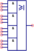
Component Data
| Field | Wert |
|---|---|
| Caption | 4x3 AndOr |
Beschreibung |
4x3 andor verilog device |
| Schematic entry | andor4x3 |
| Netlist entry | Y |
Typ |
Component |
| Bitmap file | andor4x3 |
Eigenschaften |
2 |
| Category | digital components |
Component Parameters
| Name | Wert |
Display | Beschreibung |
|---|---|---|---|
| TR | 6 | nein |
transfer function high scaling factor |
| Delay | 1 ns | nein |
output delay (s) |
4X4 Andor
Symbol
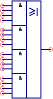
Component Data
| Field | Wert |
|---|---|
| Caption | 4x4 AndOr |
Beschreibung |
4x4 andor verilog device |
| Schematic entry | andor4x4 |
| Netlist entry | Y |
Typ |
Component |
| Bitmap file | andor4x4 |
Eigenschaften |
2 |
| Category | digital components |
Component Parameters
| Name | Wert |
Display | Beschreibung |
|---|---|---|---|
| TR | 6 | nein |
transfer function high scaling factor |
| Delay | 1 ns | nein |
output delay (s) |
2To1 Mux
Symbol
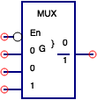
Component Data
| Field | Wert |
|---|---|
| Caption | 2to1 Mux |
Beschreibung |
2to1 multiplexer verilog device |
| Schematic entry | mux2to1 |
| Netlist entry | Y |
Typ |
Component |
| Bitmap file | mux2to1 |
Eigenschaften |
2 |
| Category | digital components |
Component Parameters
| Name | Wert |
Display | Beschreibung |
|---|---|---|---|
| TR | 6 | nein |
transfer function high scaling factor |
| Delay | 1 ns | nein |
output delay (s) |
4To1 Mux
Symbol
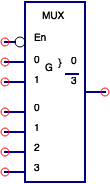
Component Data
| Field | Wert |
|---|---|
| Caption | 4to1 Mux |
Beschreibung |
4to1 multiplexer verilog device |
| Schematic entry | mux4to1 |
| Netlist entry | Y |
Typ |
Component |
| Bitmap file | mux4to1 |
Eigenschaften |
2 |
| Category | digital components |
Component Parameters
| Name | Wert |
Display | Beschreibung |
|---|---|---|---|
| TR | 6 | nein |
transfer function high scaling factor |
| Delay | 1 ns | nein |
output delay (s) |
8To1 Mux
Symbol
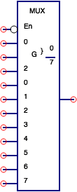
Component Data
| Field | Wert |
|---|---|
| Caption | 8to1 Mux |
Beschreibung |
8to1 multiplexer verilog device |
| Schematic entry | mux8to1 |
| Netlist entry | Y |
Typ |
Component |
| Bitmap file | mux8to1 |
Eigenschaften |
2 |
| Category | digital components |
Component Parameters
| Name | Wert |
Display | Beschreibung |
|---|---|---|---|
| TR | 6 | nein |
transfer function high scaling factor |
| Delay | 1 ns | nein |
output delay (s) |
2To4 Demux
Symbol
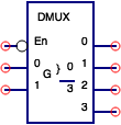
Component Data
| Field | Wert |
|---|---|
| Caption | 2to4 Demux |
Beschreibung |
2to4 demultiplexer verilog device |
| Schematic entry | dmux2to4 |
| Netlist entry | Y |
Typ |
Component |
| Bitmap file | dmux2to4 |
Eigenschaften |
2 |
| Category | digital components |
Component Parameters
| Name | Wert |
Display | Beschreibung |
|---|---|---|---|
| TR | 6 | nein |
transfer function high scaling factor |
| Delay | 1 ns | nein |
output delay (s) |
3To8 Demux
Symbol
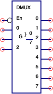
Component Data
| Field | Wert |
|---|---|
| Caption | 3to8 Demux |
Beschreibung |
3to8 demultiplexer verilog device |
| Schematic entry | dmux3to8 |
| Netlist entry | Y |
Typ |
Component |
| Bitmap file | dmux3to8 |
Eigenschaften |
2 |
| Category | digital components |
Component Parameters
| Name | Wert |
Display | Beschreibung |
|---|---|---|---|
| TR | 6 | nein |
transfer function high scaling factor |
| Delay | 1 ns | nein |
output delay (s) |
4To16 Demux
Symbol
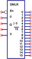
Component Data
| Field | Wert |
|---|---|
| Caption | 4to16 Demux |
Beschreibung |
4to16 demultiplexer verilog device |
| Schematic entry | dmux4to16 |
| Netlist entry | Y |
Typ |
Component |
| Bitmap file | dmux4to16 |
Eigenschaften |
2 |
| Category | digital components |
Component Parameters
| Name | Wert |
Display | Beschreibung |
|---|---|---|---|
| TR | 6 | nein |
transfer function high scaling factor |
| Delay | 1 ns | nein |
output delay (s) |
1Bit Halfadder
Symbol
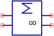
Component Data
| Field | Wert |
|---|---|
| Caption | 1Bit HalfAdder |
Beschreibung |
1bit half adder verilog device |
| Schematic entry | ha1b |
| Netlist entry | Y |
Typ |
Component |
| Bitmap file | ha1b |
Eigenschaften |
2 |
| Category | digital components |
Component Parameters
| Name | Wert |
Display | Beschreibung |
|---|---|---|---|
| TR | 6 | nein |
transfer function high scaling factor |
| Delay | 1 ns | nein |
output delay (s) |
1Bit Fulladder
Symbol
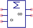
Component Data
| Field | Wert |
|---|---|
| Caption | 1Bit FullAdder |
Beschreibung |
1bit full adder verilog device |
| Schematic entry | fa1b |
| Netlist entry | Y |
Typ |
Component |
| Bitmap file | fa1b |
Eigenschaften |
2 |
| Category | digital components |
Component Parameters
| Name | Wert |
Display | Beschreibung |
|---|---|---|---|
| TR | 6 | nein |
transfer function high scaling factor |
| Delay | 1 ns | nein |
output delay (s) |
2Bit Fulladder
Symbol
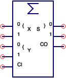
Component Data
| Field | Wert |
|---|---|
| Caption | 2Bit FullAdder |
Beschreibung |
2bit full adder verilog device |
| Schematic entry | fa2b |
| Netlist entry | Y |
Typ |
Component |
| Bitmap file | fa2b |
Eigenschaften |
2 |
| Category | digital components |
Component Parameters
| Name | Wert |
Display | Beschreibung |
|---|---|---|---|
| TR | 6 | nein |
transfer function high scaling factor |
| Delay | 1 ns | nein |
output delay (s) |
Rs-Flipflop
Symbol

Component Data
| Field | Wert |
|---|---|
| Caption | RS-Speicherglied |
Beschreibung |
RS-Speicherglied |
| Schematic entry | RSFF |
| Netlist entry | Y |
Typ |
DigitalComponent |
| Bitmap file | rsflipflop |
Eigenschaften |
1 |
| Category | digital components |
Component Parameters
| Name | Wert |
Display | Beschreibung |
|---|---|---|---|
| t | 0 | nein |
Verzögerungszeit |
D-Flipflop
Symbol

Component Data
| Field | Wert |
|---|---|
| Caption | D-Speicherglied |
Beschreibung |
D-Speicherglied mit asynchronem Reseteingang |
| Schematic entry | DFF |
| Netlist entry | Y |
Typ |
DigitalComponent |
| Bitmap file | dflipflop |
Eigenschaften |
1 |
| Category | digital components |
Component Parameters
| Name | Wert |
Display | Beschreibung |
|---|---|---|---|
| t | 0 | nein |
Verzögerungszeit |
D-Flipflop W/ Sr
Symbol
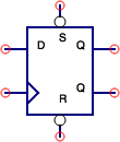
Component Data
| Field | Wert |
|---|---|
| Caption | D-FlipFlop w/ SR |
Beschreibung |
D flip flop with set and reset verilog device |
| Schematic entry | dff_SR |
| Netlist entry | Y |
Typ |
Component |
| Bitmap file | dff_SR |
Eigenschaften |
3 |
| Category | digital components |
Component Parameters
| Name | Wert |
Display | Beschreibung |
|---|---|---|---|
| TR_H | 6 | nein |
cross coupled gate transfer function high scaling factor |
| TR_L | 5 | nein |
cross coupled gate transfer function low scaling factor |
| Delay | 1 ns | nein |
cross coupled gate delay (s) |
Jk-Flipflop
Symbol

Component Data
| Field | Wert |
|---|---|
| Caption | JK-Speicherglied |
Beschreibung |
JK-Speicherglied mit asynchronen Set- und Reseteingängen |
| Schematic entry | JKFF |
| Netlist entry | Y |
Typ |
DigitalComponent |
| Bitmap file | jkflipflop |
Eigenschaften |
1 |
| Category | digital components |
Component Parameters
| Name | Wert |
Display | Beschreibung |
|---|---|---|---|
| t | 0 | nein |
Verzögerungszeit |
Jk-Flipflop W/ Sr
Symbol
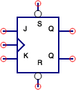
Component Data
| Field | Wert |
|---|---|
| Caption | JK-FlipFlop w/ SR |
Beschreibung |
jk flip flop with set and reset verilog device |
| Schematic entry | jkff_SR |
| Netlist entry | Y |
Typ |
Component |
| Bitmap file | jkff_SR |
Eigenschaften |
3 |
| Category | digital components |
Component Parameters
| Name | Wert |
Display | Beschreibung |
|---|---|---|---|
| TR_H | 6 | nein |
cross coupled gate transfer function high scaling factor |
| TR_L | 5 | nein |
cross coupled gate transfer function low scaling factor |
| Delay | 1 ns | nein |
cross coupled gate delay (s) |
T-Flipflop W/ Sr
Symbol
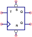
Component Data
| Field | Wert |
|---|---|
| Caption | T-FlipFlop w/ SR |
Beschreibung |
T flip flop with set and reset verilog device |
| Schematic entry | tff_SR |
| Netlist entry | Y |
Typ |
Component |
| Bitmap file | tff_SR |
Eigenschaften |
3 |
| Category | digital components |
Component Parameters
| Name | Wert |
Display | Beschreibung |
|---|---|---|---|
| TR_H | 6 | nein |
cross coupled gate transfer function high scaling factor |
| TR_L | 5 | nein |
cross coupled gate transfer function low scaling factor |
| Delay | 1 ns | nein |
cross coupled gate delay (s) |
Gated D-Latch
Symbol
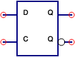
Component Data
| Field | Wert |
|---|---|
| Caption | Gated D-Latch |
Beschreibung |
gated D latch verilog device |
| Schematic entry | gatedDlatch |
| Netlist entry | Y |
Typ |
Component |
| Bitmap file | gatedDlatch |
Eigenschaften |
3 |
| Category | digital components |
Component Parameters
| Name | Wert |
Display | Beschreibung |
|---|---|---|---|
| TR_H | 6 | nein |
cross coupled gate transfer function high scaling factor |
| TR_L | 5 | nein |
cross coupled gate transfer function low scaling factor |
| Delay | 1 ns | nein |
cross coupled gate delay (s) |
Logic 0
Symbol

Component Data
| Field | Wert |
|---|---|
| Caption | Logic 0 |
Beschreibung |
logic 0 verilog device |
| Schematic entry | logic_0 |
| Netlist entry | S |
Typ |
Component |
| Bitmap file | logic_0 |
Eigenschaften |
1 |
| Category | digital components |
Component Parameters
| Name | Wert |
Display | Beschreibung |
|---|---|---|---|
| LEVEL | 0 | nein |
logic 0 voltage level (V) |
Logic 1
Symbol

Component Data
| Field | Wert |
|---|---|
| Caption | Logic 1 |
Beschreibung |
logic 1 verilog device |
| Schematic entry | logic_1 |
| Netlist entry | S |
Typ |
Component |
| Bitmap file | logic_1 |
Eigenschaften |
1 |
| Category | digital components |
Component Parameters
| Name | Wert |
Display | Beschreibung |
|---|---|---|---|
| LEVEL | 1 | nein |
logic 1 voltage level (V) |
2Bit Pattern
Symbol
Component Data
| Field | Wert |
|---|---|
| Caption | 2Bit Pattern |
Beschreibung |
2bit pattern generator verilog device |
| Schematic entry | pad2bit |
| Netlist entry | Y |
Typ |
Component |
| Bitmap file | pad2bit |
Eigenschaften |
1 |
| Category | digital components |
Component Parameters
| Name | Wert |
Display | Beschreibung |
|---|---|---|---|
| Number | 0 | nein |
pad output value |
3Bit Pattern
Symbol
Component Data
| Field | Wert |
|---|---|
| Caption | 3Bit Pattern |
Beschreibung |
3bit pattern generator verilog device |
| Schematic entry | pad3bit |
| Netlist entry | Y |
Typ |
Component |
| Bitmap file | pad3bit |
Eigenschaften |
1 |
| Category | digital components |
Component Parameters
| Name | Wert |
Display | Beschreibung |
|---|---|---|---|
| Number | 0 | nein |
pad output value |
4Bit Pattern
Symbol
Component Data
| Field | Wert |
|---|---|
| Caption | 4Bit Pattern |
Beschreibung |
4bit pattern generator verilog device |
| Schematic entry | pad4bit |
| Netlist entry | Y |
Typ |
Component |
| Bitmap file | pad4bit |
Eigenschaften |
1 |
| Category | digital components |
Component Parameters
| Name | Wert |
Display | Beschreibung |
|---|---|---|---|
| Number | 0 | nein |
pad output value |
A2D Level Shifter
Symbol

Component Data
| Field | Wert |
|---|---|
| Caption | A2D Level Shifter |
Beschreibung |
data voltage level shifter (analogue to digital) verilog device |
| Schematic entry | DLS_nto1 |
| Netlist entry | Y |
Typ |
AnalogComponent |
| Bitmap file | DLS_nto1 |
Eigenschaften |
2 |
| Category | digital components |
Component Parameters
| Name | Wert |
Display | Beschreibung |
|---|---|---|---|
| LEVEL | 5 V | nein |
voltage level (V) |
| Delay | 1 ns | nein |
time delay (s) |
D2A Level Shifter
Symbol

Component Data
| Field | Wert |
|---|---|
| Caption | D2A Level Shifter |
Beschreibung |
data voltage level shifter (digital to analogue) verilog device |
| Schematic entry | DLS_1ton |
| Netlist entry | Y |
Typ |
AnalogComponent |
| Bitmap file | DLS_1ton |
Eigenschaften |
2 |
| Category | digital components |
Component Parameters
| Name | Wert |
Display | Beschreibung |
|---|---|---|---|
| LEVEL | 5 V | nein |
voltage level |
| Delay | 1 ns | nein |
time delay (s) |
4Bit Bin2Grey
Symbol

Component Data
| Field | Wert |
|---|---|
| Caption | 4Bit Bin2Grey |
Beschreibung |
4bit binary to grey converter verilog device |
| Schematic entry | binarytogrey4bit |
| Netlist entry | Y |
Typ |
Component |
| Bitmap file | binarytogrey4bit |
Eigenschaften |
2 |
| Category | digital components |
Component Parameters
| Name | Wert |
Display | Beschreibung |
|---|---|---|---|
| TR | 6 | nein |
transfer function scaling factor |
| Delay | 1 ns | nein |
output delay (s) |
4Bit Grey2Bin
Symbol
Component Data
| Field | Wert |
|---|---|
| Caption | 4Bit Grey2Bin |
Beschreibung |
4bit grey to binary converter verilog device |
| Schematic entry | greytobinary4bit |
| Netlist entry | Y |
Typ |
Component |
| Bitmap file | greytobinary4bit |
Eigenschaften |
2 |
| Category | digital components |
Component Parameters
| Name | Wert |
Display | Beschreibung |
|---|---|---|---|
| TR | 6 | nein |
transfer function scaling factor |
| Delay | 1 ns | nein |
output delay (s) |
1Bit Comparator
Symbol
Component Data
| Field | Wert |
|---|---|
| Caption | 1Bit Comparator |
Beschreibung |
1bit comparator verilog device |
| Schematic entry | comp_1bit |
| Netlist entry | Y |
Typ |
Component |
| Bitmap file | comp_1bit |
Eigenschaften |
2 |
| Category | digital components |
Component Parameters
| Name | Wert |
Display | Beschreibung |
|---|---|---|---|
| TR | 6 | nein |
transfer function high scaling factor |
| Delay | 1 ns | nein |
output delay (s) |
2Bit Comparator
Symbol
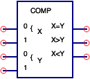
Component Data
| Field | Wert |
|---|---|
| Caption | 2Bit Comparator |
Beschreibung |
2bit comparator verilog device |
| Schematic entry | comp_2bit |
| Netlist entry | Y |
Typ |
Component |
| Bitmap file | comp_2bit |
Eigenschaften |
2 |
| Category | digital components |
Component Parameters
| Name | Wert |
Display | Beschreibung |
|---|---|---|---|
| TR | 6 | nein |
transfer function high scaling factor |
| Delay | 1 ns | nein |
output delay (s) |
4Bit Comparator
Symbol
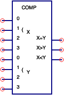
Component Data
| Field | Wert |
|---|---|
| Caption | 4Bit Comparator |
Beschreibung |
4bit comparator verilog device |
| Schematic entry | comp_4bit |
| Netlist entry | Y |
Typ |
Component |
| Bitmap file | comp_4bit |
Eigenschaften |
2 |
| Category | digital components |
Component Parameters
| Name | Wert |
Display | Beschreibung |
|---|---|---|---|
| TR | 6 | nein |
transfer function high scaling factor |
| Delay | 1 ns | nein |
output delay (s) |
4Bit Hpri-Bin
Symbol
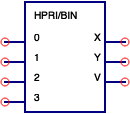
Component Data
| Field | Wert |
|---|---|
| Caption | 4Bit HPRI-Bin |
Beschreibung |
4bit highest priority encoder (binary form) verilog device |
| Schematic entry | hpribin4bit |
| Netlist entry | Y |
Typ |
Component |
| Bitmap file | hpribin4bit |
Eigenschaften |
2 |
| Category | digital components |
Component Parameters
| Name | Wert |
Display | Beschreibung |
|---|---|---|---|
| TR | 6 | nein |
transfer function scaling factor |
| Delay | 1 ns | nein |
output delay (s) |
Vhdl File
Symbol

Component Data
| Field | Wert |
|---|---|
| Caption | VHDL file |
Beschreibung |
VHDL file |
| Schematic entry | VHDL |
| Netlist entry | X |
Typ |
DigitalComponent |
| Bitmap file | vhdlfile |
Eigenschaften |
1 |
| Category | digital components |
Component Parameters
| Name | Wert |
Display | Beschreibung |
|---|---|---|---|
Datei |
sub.vhdl | nein |
Name of VHDL file |
Verilog File
Symbol
Component Data
| Field | Wert |
|---|---|
| Caption | Verilog file |
Beschreibung |
Verilog file |
| Schematic entry | Verilog |
| Netlist entry | X |
Typ |
DigitalComponent |
| Bitmap file | vhdlfile |
Eigenschaften |
1 |
| Category | digital components |
Component Parameters
| Name | Wert |
Display | Beschreibung |
|---|---|---|---|
Datei |
sub.v | nein |
Name of Verilog file |
Digital Simulation
Symbol

Component Data
| Field | Wert |
|---|---|
| Caption | Digitalsimulation |
Beschreibung |
Digitalsimulation |
| Schematic entry | .Digi |
| Netlist entry | Digi |
Typ |
DigitalComponent |
| Bitmap file | digi |
Eigenschaften |
3 |
| Category | digital components |
Component Parameters
| Name | Wert |
Display | Beschreibung |
|---|---|---|---|
Typ |
TruthTable | ja |
type of simulation [TruthTable, TimeList] |
| time | 10 ns | nein |
Zeitdauer der TimeList Simulation |
| Model | VHDL | nein |
netlist format [VHDL, Verilog] |
File Components
Spice Netlist
Symbol

Component Data
| Field | Wert |
|---|---|
| Caption | SPICE Netzliste |
Beschreibung |
SPICE Netzlistendatei |
| Schematic entry | SPICE |
| Netlist entry | X |
Typ |
AnalogComponent |
| Bitmap file | spicefile |
Eigenschaften |
4 |
| Category | file components |
Component Parameters
| Name | Wert |
Display | Beschreibung |
|---|---|---|---|
Datei |
ja |
x | |
| Ports | nein |
x | |
| Sim | ja |
nein |
x |
| Preprocessor | none | nein |
x |
1-Port S Parameter File
Symbol

Component Data
| Field | Wert |
|---|---|
| Caption | 1-Tor S-Parameter Datei |
Beschreibung |
S-Parameter Datei |
| Schematic entry | SPfile |
| Netlist entry | X |
Typ |
AnalogComponent |
| Bitmap file | spfile1 |
Eigenschaften |
5 |
| Category | file components |
Component Parameters
| Name | Wert |
Display | Beschreibung |
|---|---|---|---|
Datei |
test.s1p | ja |
Name der S-Parameter Datei |
Daten |
rectangular | nein |
data type [rectangular, polar] |
| Interpolator | linear | nein |
interpolation type [linear, cubic] |
| duringDC | open | nein |
representation during DC analysis [open, short, shortall, unspecified] |
| Ports | 1 | nein |
Anzahl der Tore |
2-Port S Parameter File
Symbol

Component Data
| Field | Wert |
|---|---|
| Caption | 2-Tor S-Parameter Datei |
Beschreibung |
S-Parameter Datei |
| Schematic entry | SPfile |
| Netlist entry | X |
Typ |
AnalogComponent |
| Bitmap file | spfile2 |
Eigenschaften |
5 |
| Category | file components |
Component Parameters
| Name | Wert |
Display | Beschreibung |
|---|---|---|---|
Datei |
test.s2p | ja |
Name der S-Parameter Datei |
Daten |
rectangular | nein |
data type [rectangular, polar] |
| Interpolator | linear | nein |
interpolation type [linear, cubic] |
| duringDC | open | nein |
representation during DC analysis [open, short, shortall, unspecified] |
| Ports | 2 | nein |
Anzahl der Tore |
N-Port S Parameter File
Symbol
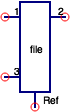
Component Data
| Field | Wert |
|---|---|
| Caption | n-Tor S-Parameter Datei |
Beschreibung |
S-Parameter Datei |
| Schematic entry | SPfile |
| Netlist entry | X |
Typ |
AnalogComponent |
| Bitmap file | spfile3 |
Eigenschaften |
5 |
| Category | file components |
Component Parameters
| Name | Wert |
Display | Beschreibung |
|---|---|---|---|
Datei |
test.s3p | ja |
Name der S-Parameter Datei |
Daten |
rectangular | nein |
data type [rectangular, polar] |
| Interpolator | linear | nein |
interpolation type [linear, cubic] |
| duringDC | open | nein |
representation during DC analysis [open, short, shortall, unspecified] |
| Ports | 3 | nein |
Anzahl der Tore |
Schaltkreis
Symbol

Component Data
| Field | Wert |
|---|---|
| Caption | Schaltkreis |
Beschreibung |
Teilschaltung |
| Schematic entry | Sub |
| Netlist entry | SUB |
Typ |
Component |
| Bitmap file | Teilschaltung |
Eigenschaften |
1 |
| Category | file components |
Component Parameters
| Name | Wert |
Display | Beschreibung |
|---|---|---|---|
Datei |
nein |
Name der Qucs Schaltplandatei |
Simulations
Dc Simulation
Symbol

Component Data
| Field | Wert |
|---|---|
| Caption | DC-Simulation |
Beschreibung |
DC-Simulation |
| Schematic entry | .DC |
| Netlist entry | DC |
Typ |
AnalogComponent |
| Bitmap file | dc |
Eigenschaften |
9 |
| Category | simulations |
Component Parameters
| Name | Wert |
Display | Beschreibung |
|---|---|---|---|
| Temp | 26.85 | nein |
Simulationstemperatur in °C |
| reltol | 0.001 | nein |
relative Toleranz für Konvergenz |
| abstol | 1 pA | nein |
absolute Toleranz für Ströme |
| vntol | 1 uV | nein |
absolute Toleranz für Spannungen |
| saveOPs | nein |
nein |
put operating points into dataset [yes, no] |
| MaxIter | 150 | nein |
maximale Anzahl der Iterationen |
| saveAll | nein |
nein |
save subcircuit nodes into dataset [yes, no] |
| convHelper | none | nein |
preferred convergence algorithm [none, gMinStepping, SteepestDescent, LineSearch, Attenuation, SourceStepping] |
| Solver | CroutLU | nein |
method for solving the circuit matrix [CroutLU, DoolittleLU, HouseholderQR, HouseholderLQ, GolubSVD] |
Transient Simulation
Symbol

Component Data
| Field | Wert |
|---|---|
| Caption | Transientsimulation |
Beschreibung |
Transientsimulation |
| Schematic entry | .TR |
| Netlist entry | TR |
Typ |
AnalogComponent |
| Bitmap file | tran |
Eigenschaften |
20 |
| Category | simulations |
Component Parameters
| Name | Wert |
Display | Beschreibung |
|---|---|---|---|
Typ |
lin | ja |
sweep type [lin, log, list, const] |
| Start | 0 | ja |
Startzeit in Sekunden |
| Stop | 1 ms | ja |
Stopzeit in Sekunden |
| Points | 11 | nein |
Anzahl der Simulationszeitschritte |
| IntegrationMethod | Trapezoidal | nein |
integration method [Euler, Trapezoidal, Gear, AdamsMoulton] |
| Order | 2 | nein |
order of integration method (1-6) |
| InitialStep | 1 ns | nein |
Anfangsschrittweite in Sekunden |
| MinStep | 1e-16 | nein |
minimale Schrittweite in Sekunden |
| MaxIter | 150 | nein |
maximale Anzahl der Iterationen |
| reltol | 0.001 | nein |
relative Toleranz für Konvergenz |
| abstol | 1 pA | nein |
absolute Toleranz für Ströme |
| vntol | 1 uV | nein |
absolute Toleranz für Spannungen |
| Temp | 26.85 | nein |
Simulationstemperatur in °C |
| LTEreltol | 1e-3 | nein |
relative Toleranz des lokalen Abbruchfehlers |
| LTEabstol | 1e-6 | nein |
absolute Toleranz des lokalen Abbruchfehlers |
| LTEfactor | 1 | nein |
Faktor für die Überbewertung des lokalen Abbruchfehlers |
| Solver | CroutLU | nein |
method for solving the circuit matrix [CroutLU, DoolittleLU, HouseholderQR, HouseholderLQ, GolubSVD] |
| relaxTSR | nein |
nein |
relax time step raster [no, yes] |
| initialDC | ja |
nein |
perform an initial DC analysis [yes, no] |
| MaxStep | 0 | nein |
maximum step size in seconds |
Ac Simulation
Symbol

Component Data
| Field | Wert |
|---|---|
| Caption | AC-Simulation |
Beschreibung |
AC-Simulation |
| Schematic entry | .AC |
| Netlist entry | AC |
Typ |
AnalogComponent |
| Bitmap file | ac |
Eigenschaften |
5 |
| Category | simulations |
Component Parameters
| Name | Wert |
Display | Beschreibung |
|---|---|---|---|
Typ |
lin | ja |
sweep type [lin, log, list, const] |
| Start | 1 GHz | ja |
Startfrequenz in Hertz |
| Stop | 10 GHz | ja |
Stopfrequenz in Hertz |
| Points | 19 | ja |
Anzahl der Simulationsschritte |
| Noise | nein |
nein |
calculate noise voltages [yes, no] |
S-Parameter Simulation
Symbol

Component Data
| Field | Wert |
|---|---|
| Caption | S-Parameter Simulation |
Beschreibung |
S-Parameter Simulation |
| Schematic entry | .SP |
| Netlist entry | SP |
Typ |
AnalogComponent |
| Bitmap file | sparameter |
Eigenschaften |
9 |
| Category | simulations |
Component Parameters
| Name | Wert |
Display | Beschreibung |
|---|---|---|---|
Typ |
lin | ja |
sweep type [lin, log, list, const] |
| Start | 1 GHz | ja |
Startfrequenz in Hertz |
| Stop | 10 GHz | ja |
Stopfrequenz in Hertz |
| Points | 19 | ja |
Anzahl der Simulationsschritte |
| Noise | nein |
nein |
calculate noise parameters [yes, no] |
| NoiseIP | 1 | nein |
Eingangstor für die Rauschzahl |
| NoiseOP | 2 | nein |
Ausgangstor für die Rauschzahl |
| saveCVs | nein |
nein |
put characteristic values into dataset [yes, no] |
| saveAll | nein |
nein |
save subcircuit characteristic values into dataset [yes, no] |
Harmonic Balance
Symbol

Component Data
| Field | Wert |
|---|---|
| Caption | Harmonic balance |
Beschreibung |
Harmonic balance simulation |
| Schematic entry | .HB |
| Netlist entry | HB |
Typ |
AnalogComponent |
| Bitmap file | hb |
Eigenschaften |
6 |
| Category | simulations |
Component Parameters
| Name | Wert |
Display | Beschreibung |
|---|---|---|---|
| f | 1 GHz | nein |
Frequenz in Hertz |
| n | 4 | ja |
Anzahl der Harmonischen |
| iabstol | 1 pA | nein |
absolute Toleranz für Ströme |
| vabstol | 1 uV | nein |
absolute Toleranz für Spannungen |
| reltol | 0.001 | nein |
relative Toleranz für Konvergenz |
| MaxIter | 150 | nein |
maximale Anzahl der Iterationen |
Parameter Sweep
Symbol

Component Data
| Field | Wert |
|---|---|
| Caption | Parameterdurchlauf |
Beschreibung |
Parameterdurchlauf |
| Schematic entry | .SW |
| Netlist entry | SW |
Typ |
AnalogComponent |
| Bitmap file | sweep |
Eigenschaften |
6 |
| Category | simulations |
Component Parameters
| Name | Wert |
Display | Beschreibung |
|---|---|---|---|
| Sim | ja |
Simulation für den Parameterdurchlauf |
|
Typ |
lin | ja |
sweep type [lin, log, list, const] |
| Param | R1 | ja |
Durchlaufvariable |
| Start | 5 Ohm | ja |
Startwert des Durchlaufs |
| Stop | 50 Ohm | ja |
Stopwert des Durchlaufs |
| Points | 20 | ja |
Anzahl der Simulationsschritte |
Digital Simulation
Symbol
Component Data
| Field | Wert |
|---|---|
| Caption | Digitalsimulation |
Beschreibung |
Digitalsimulation |
| Schematic entry | .Digi |
| Netlist entry | Digi |
Typ |
DigitalComponent |
| Bitmap file | digi |
Eigenschaften |
3 |
| Category | simulations |
Component Parameters
| Name | Wert |
Display | Beschreibung |
|---|---|---|---|
Typ |
TruthTable | ja |
type of simulation [TruthTable, TimeList] |
| time | 10 ns | nein |
Zeitdauer der TimeList Simulation |
| Model | VHDL | nein |
netlist format [VHDL, Verilog] |
Optimization
Symbol

Component Data
| Field | Wert |
|---|---|
| Caption | optimization |
Beschreibung |
Optimization |
| Schematic entry | .Opt |
| Netlist entry | Opt |
Typ |
AnalogComponent |
| Bitmap file | optimize |
Eigenschaften |
2 |
| Category | simulations |
Component Parameters
| Name | Wert |
Display | Beschreibung |
|---|---|---|---|
| Sim | nein |
||
| DE | 3|50|2|20|0.85|1|3|1e-6|10|100 | nein |