![\includegraphics[width=4cm]{opamp}](img1207.png)
|
The ideal operational amplifier, as shown in fig. 10.1, is determined by the following equation which introduces one more unknown in the MNA matrix.
The new unknown variable ![]() must be considered by the three
remaining simple equations.
must be considered by the three
remaining simple equations.
| (10.2) |
And in matrix representation this is (for DC and AC simulation):
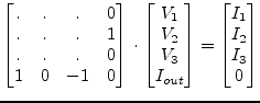 |
(10.3) |
The operational amplifier could be considered as a special case of a
voltage controlled current source with infinite forward
transconductance ![]() . Please note that the presented matrix form is
only valid in cases where there is a finite feedback impedance
between the output and the inverting input port.
. Please note that the presented matrix form is
only valid in cases where there is a finite feedback impedance
between the output and the inverting input port.
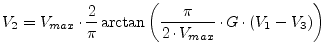
To allow a feedback circuit to the non-inverting input (e.g. for a Schmitt trigger), one needs a limited output voltage swing. The following equations are often used to model the transmission characteristic of operational amplifiers.
| (10.4) |
with ![]() being the maximum output voltage swing and
being the maximum output voltage swing and ![]() the
voltage amplification. To model the small-signal behaviour (AC
analysis), it is necessary to differentiate:
the
voltage amplification. To model the small-signal behaviour (AC
analysis), it is necessary to differentiate:
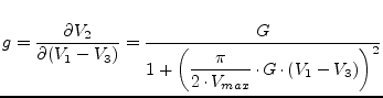 |
(10.6) |
This leads to the following matrix representation being a specialised
three node voltage controlled voltage source (see section
9.19.3 on page ![[*]](crossref.png) ).
).
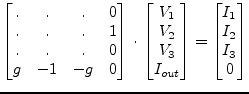 |
(10.7) |
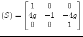
The above MNA matrix entries are also used during the non-linear DC analysis with the 0 in the right hand side vector replaced by an equivalent voltage
| (10.8) |
With the given small-signal matrix representation, building the S-parameters is easy.
 |
(10.9) |