![\includegraphics[width=10cm]{NLexample}](img304.png)
|
Previous sections described using the modified nodal analysis solving linear networks including controlled sources. It can also be used to solve networks with non-linear components like diodes and transistors. Most methods are based on iterative solutions of a linearised equation system. The best known is the so called Newton-Raphson method.
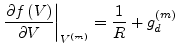
The Newton-Raphson method is going to be introduced using the example circuit shown in fig. 3.2 having a single unknown: the voltage at node 1.
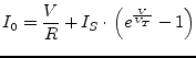
The 1x1 MNA equation system to be solved can be written as
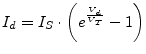
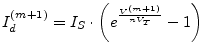
whereas the value for ![]() is now going to be explained. The current
through a diode is simply determined by Schockley's approximation
is now going to be explained. The current
through a diode is simply determined by Schockley's approximation
 |
(3.24) |
Thus Kirchhoff's current law at node 1 can be expressed as
 |
(3.25) |
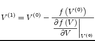
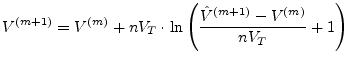
By establishing eq. (3.26) it is possible to trace the
problem back to finding the zero point of the function ![]() .
.
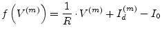
Newton developed a method stating that the zero point of a functions
derivative (i.e. the tangent) at a given point is nearer to the zero
point of the function itself than the original point. In mathematical
terms this means to linearise the function ![]() at a starting value
at a starting value
![]() .
.
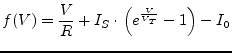
Setting
![]() gives
gives
 |
(3.28) |
or in the general case with ![]() being the number of iteration
being the number of iteration
This must be computed until ![]() and
and ![]() differ less than a
certain barrier.
differ less than a
certain barrier.
With very small
![]() the iteration would break too
early and for little
the iteration would break too
early and for little
![]() values the iteration aims to
a useless precision for large absolute values of
values the iteration aims to
a useless precision for large absolute values of ![]() .
.
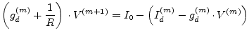
With this theoretical background it is now possible to step back to eq. (3.26) being the determining equation for the example circuit. With
 |
(3.31) |
and
 |
(3.32) |
the eq. (3.29) can be written as
when the expression
 |
(3.34) |
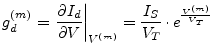
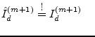
based upon eq. (3.26) is taken into account. Comparing the introductory MNA equation system in eq. (3.23) with eq. (3.33) proposes the following equivalent circuit for the diode model.
With
| (3.35) |
the MNA matrix entries can finally be written as
 |
(3.36) |
In analog ways all controlled current sources with non-linear
current-voltage dependency built into diodes and transistors can be
modeled. The left hand side of the MNA matrix (the A matrix) is
called Jacobian matrix which is going to be build in each iteration
step. For the solution vector ![]() possibly containing currents as
well when voltage sources are in place a likely convergence criteria
as defined in eq. (3.30) must be defined for the
currents.
possibly containing currents as
well when voltage sources are in place a likely convergence criteria
as defined in eq. (3.30) must be defined for the
currents.
Having understood the one-dimensional example, it is now only a
small step to the general multi-dimensional algorithm: The node
voltage becomes a vector
![]() , factors become
the corresponding matrices and differentiations become Jacobian
matrices.
, factors become
the corresponding matrices and differentiations become Jacobian
matrices.
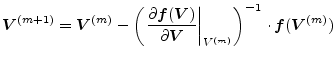
The function whose zero must be found is the transformed MNA equation 3.23:
| (3.37) |
The only difference to the linear case is that the vector
![]() also contains the currents flowing out of the non-linear components.
The iteration formula of the Newton-Raphson method writes:
also contains the currents flowing out of the non-linear components.
The iteration formula of the Newton-Raphson method writes:
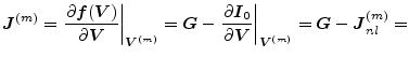
Note that the Jacobian matrix is nothing else but the real part of the MNA matrix for the AC analysis:
where the index ![]() denotes only the non-linear terms. Putting equation
3.39 into equation 3.38 and multiplying it
with the Jacobian matrix leads to
denotes only the non-linear terms. Putting equation
3.39 into equation 3.38 and multiplying it
with the Jacobian matrix leads to
| (3.40) | ||
| (3.41) | ||
| (3.42) |
So, bringing the Jacobian back to the right side results in the new iteration formula:
 |
(3.43) |
The negative sign in front of
![]() is due to the
definition of
is due to the
definition of
![]() flowing out of the component. Note
that
flowing out of the component. Note
that
![]() still contains contributions of linear
and non-linear current sources.
still contains contributions of linear
and non-linear current sources.
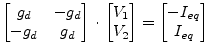
Numerical as well as convergence problems occur during the Newton-Raphson iterations when dealing with non-linear device curves as they are used to model the DC behaviour of diodes and transistors.
Linearising the exponential diode eq. (3.48) in the forward
region a numerical overflow can occur. The diagram in
fig. 3.5 visualises this situation. Starting with
![]() the next iteration value gets
the next iteration value gets ![]() which results in an
indefinite large diode current. It can be limited by iterating in
current instead of voltage when the computed voltage exceeds a certain
value.
which results in an
indefinite large diode current. It can be limited by iterating in
current instead of voltage when the computed voltage exceeds a certain
value.
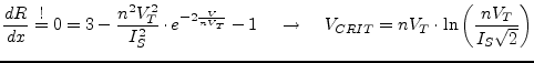
How this works is going to be explained using the diode model shown in fig. 3.4. When iterating in voltage (as normally done) the new diode current is
| (3.44) |
The computed value
![]() in iteration step
in iteration step ![]() is not
going to be used for the following step when
is not
going to be used for the following step when ![]() exceeds the
critical voltage
exceeds the
critical voltage ![]() which gets explained in the below
paragraphs. Instead, the value resulting from
which gets explained in the below
paragraphs. Instead, the value resulting from
 |
(3.45) |
is used (i.e. iterating in current). With
 and and 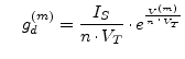 |
(3.46) |
the new voltage can be written as
 |
(3.47) |
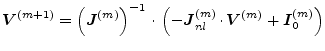
Proceeding from Shockley's simplified diode equation the critical voltage is going to be defined. The explained algorithm can be used for all exponential DC equations used in diodes and transistors.
The critical voltage ![]() is the voltage where the curve radius
of eq. (3.48) has its minimum with
is the voltage where the curve radius
of eq. (3.48) has its minimum with ![]() and
and ![]() having
equally units. The curve radius
having
equally units. The curve radius ![]() for the explicit definition in
eq. (3.49) can be written as
for the explicit definition in
eq. (3.49) can be written as
Finding this equations minimum requires the derivative.
The diagram in fig. 3.6 shows the graphs of
eq. (3.50) and eq. (3.51) with ![]() ,
,
![]() and
and
![]() .
.
With the following higher derivatives of eq. (3.48)
 |
 |
(3.52) |
 |
 |
(3.53) |
 |
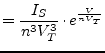 |
(3.54) |
the critical voltage results in
 |
(3.55) |
In order to avoid numerical errors a minimum value of the
pn-junction's derivative (i.e. the currents tangent in the operating
point) ![]() is defined. On the one hand this avoids very large
deviations of the appropriate voltage in the next iteration step in
the backward region of the pn-junction and on the other hand it avoids
indefinite large voltages if
is defined. On the one hand this avoids very large
deviations of the appropriate voltage in the next iteration step in
the backward region of the pn-junction and on the other hand it avoids
indefinite large voltages if ![]() itself suffers from numerical
errors and approaches zero.
itself suffers from numerical
errors and approaches zero.
The quadratic input I-V curve of field-effect transistors as well as
the output characteristics of these devices can be handled in similar
ways. The limiting (and thereby improving the convergence behaviour)
algorithm must somehow ensure that the current and/or voltage
deviation from one iteration step to the next step is not too a large
value. Because of the wide range of existing variations how these
curves are exactly modeled there is no standard strategy to achieve
this. Anyway, the threshold voltage ![]() should play an important
role as well as the direction which the current iteration step
follows.
should play an important
role as well as the direction which the current iteration step
follows.
 with
with 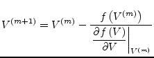
![\includegraphics[width=0.75\linewidth]{newton}](img323.png)
![\includegraphics[width=0.2\linewidth]{newtondiode}](img328.png)
 Re
Re![\includegraphics[width=0.75\linewidth]{newtonbad}](img358.png)
![\includegraphics[width=0.7\linewidth]{radius}](img366.png)