The most useful model of a microstrip cross have been published in
[39,40]. Fig. 11.10 shows the equivalent
circuit (right-hand side) and the scheme with dimensions (left-hand
side). The hatched area in the scheme marks the area modeled by the
equivalent circuit. As can be seen the model require the microstrip
width of line 1 and 3, as well as the one of line 2 and 4 to equal
each other. Furthermore the permittivity of the substrat must be
![]() . The component values are calculated as follows:
. The component values are calculated as follows:
The equation of ![]() is obtained from the one of
is obtained from the one of ![]() by
exchanging the indices (
by
exchanging the indices (![]() and
and ![]() ). Note that
). Note that ![]() is
negative, so the model is unphysical without external microstrip
lines. The above-mentioned equations are accurate to within 5%
for
is
negative, so the model is unphysical without external microstrip
lines. The above-mentioned equations are accurate to within 5%
for
![]() and
and
![]() (value of
(value of
![]() ) or for
) or for
![]() (value of
(value of
![]() ), respectively.
), respectively.
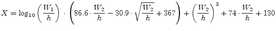
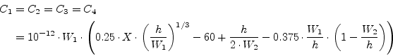
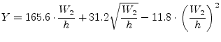
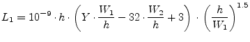
Some improvement should be added to the original model:
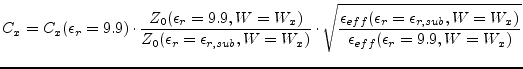 |
(11.231) |
A useful model for an unsymmetrical cross junction has never been
published. Nonetheless, as long as the lines that lie opposite are not
to different in width, the model described here can be used as a first
order approximation. This is perfomred by replacing ![]() and
and ![]() by the
arithmetic mean of the line widths that lie opposite. This is done:
by the
arithmetic mean of the line widths that lie opposite. This is done:
Another closed-form expression describing the non-ideal behaviour of a microstrip cross junction was published by [41]. Additionally there have been published papers [42,43,44] giving analytic (but not closed-form) expressions or just simple equivalent circuits with only a few expressions for certain topologies and dielectric constants which are actually of no pratical use.

![\includegraphics[width=9cm]{mscross}](img2405.png)