![\includegraphics[width=9cm]{msvia}](img2409.png)
|
According to Marc E. Goldfarb and Robert A. Pucel [45] a
via hole ground in microstrip is a series of a resistance and an
inductance. The given model for a cylindrical via hole has been
verified numerically and experimentally for a range of
![]() .
.
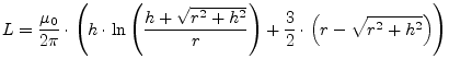 |
(11.232) |
whence ![]() is the via length (substrate height) and
is the via length (substrate height) and ![]() the
via's radius.
the
via's radius.
 |
(11.233) |
| (11.234) |
The relationship for the via resistance can be used as a close
approximation and is valid independent of the ratio of the
metalization thickness ![]() to the skin depth. In the formula
to the skin depth. In the formula ![]() denotes the specific resistance of the conductor material.
denotes the specific resistance of the conductor material.